Array
(
    [content] => 
    [params] => Array
        (
            [0] => /forum/index.php?threads/what-comes-next-after-shrink-ends.17885/
        )

    [addOns] => Array
        (
            [DL6/MLTP] => 13
            [Hampel/TimeZoneDebug] => 1000070
            [SV/ChangePostDate] => 2010200
            [SemiWiki/Newsletter] => 1000010
            [SemiWiki/WPMenu] => 1000010
            [SemiWiki/XPressExtend] => 1000010
            [ThemeHouse/XLink] => 1000970
            [ThemeHouse/XPress] => 1010570
            [XF] => 2021370
            [XFI] => 1050270
        )

    [wordpress] => /var/www/html
)

What comes next after shrink ends?

Arthur Hanson

Well-known member
With shrink reaching it physical limits what will be the next areas for advancing computational power and speed? Will TSM still be the leader in five years? Are optical chips on the horizon or will they remain a scientific curiosity? Will cost be the next area of competition as shrink ends? Also, any thoughts on the cost/performance factors of newer technologies would be appreciated.
 
Probably chiplets, wafer-scale designs, '3D' stacked designs, and so on. I believe IBM did a lot of work trying to make real products with exotic designs. I know about their System 390 'TCM' processor through a teardown video on youtube but other folks likely know more.

My hunch is it's possible to deliver another 10x in perf/$ at least, though perhaps not in perf/Watt.
 
I'm thinking they'll be paying even more attention to other elements besides silicon. As long as silicon has legs, it's been hard for other elements to be feasible, but when it runs out of steam, you may see other substances used in greater amounts and scenarios.

But, the real answer is, software. Software is so damn sloppy right now, there's a huge opportunity for performance improvement there. As we used to say "What Intel giveth, Microsoft taketh away". But, when Intel (used loosely to define hardware in general) stops giving so much, MIcrosoft (you get the point) won't have the opportunity to be so sloppy and wasteful.

There's still a lot of potential for improvement in performance, both with other materials become economically feasible, and more efficient software. We're not near the end.
Apple's tight integration and optimization has shown that there's room for multi-year leads in system efficiency just from tight hardware-software optimization.
 
According to TSMC:

Remember, N2 is nanosheets, which, unlike FinFETs, is not open source technology so this is really going to be a challenge for design and the supporting ecosystem which gives TSMC a very strong advantage. TSMC also mentioned what follows nanosheets which I found quite interesting. I’m sure we will hear more about this at IEDM 2023:

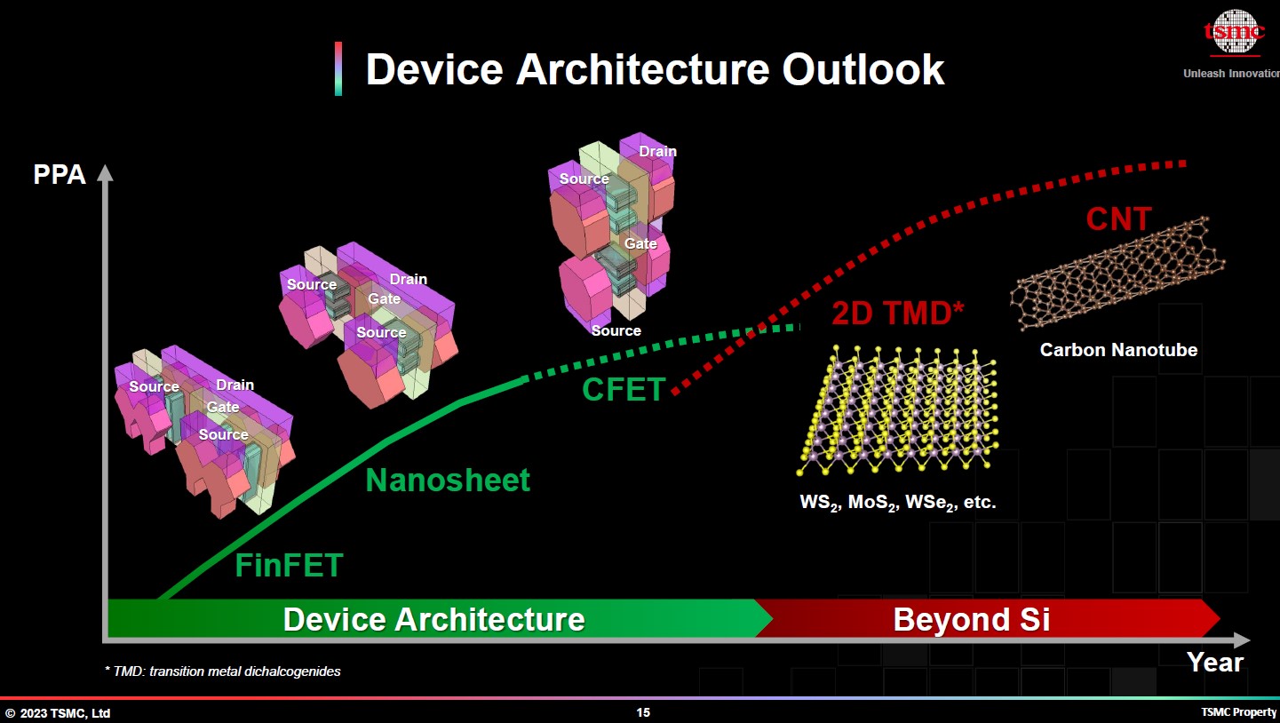
TSMC Device Architecture Outlook 2023


  • Transistor architecture has evolved from planar to FinFET and is about to change again to nanosheet.
  • Beyond nanosheet, TSMC sees vertically stacked NMOS and PMOS, known as CFET, as one of the key process architecture choices going forward.
    • TSMC estimates the density gain would fall between 5 to 2X after factoring in routing and process complexity.
  • Beyond CFET, TSMC made breakthroughs in low dimensional materials such as carbon nanotubes and 2D materials which could enable further dimensional and energy scaling.
Can you explain why this would be a such a big advantage for TSMC?
 
According to TSMC:

Remember, N2 is nanosheets, which, unlike FinFETs, is not open source technology so this is really going to be a challenge for design and the supporting ecosystem which gives TSMC a very strong advantage. TSMC also mentioned what follows nanosheets which I found quite interesting. I’m sure we will hear more about this at IEDM 2023:

TSMC Device Architecture Outlook 2023


  • Transistor architecture has evolved from planar to FinFET and is about to change again to nanosheet.
  • Beyond nanosheet, TSMC sees vertically stacked NMOS and PMOS, known as CFET, as one of the key process architecture choices going forward.
    • TSMC estimates the density gain would fall between 5 to 2X after factoring in routing and process complexity.
  • Beyond CFET, TSMC made breakthroughs in low dimensional materials such as carbon nanotubes and 2D materials which could enable further dimensional and energy scaling.
Backside power delivery, AI remastering, pattern shaping technology, and probably several other complimentary techniques/approaches will also increase density.
 
Can you explain why this would be a such a big advantage for TSMC?

Yes. TSMC has a huge ecosystem to help them with new technologies. On the design side there is the EDA and IP companies. TSMC is always first on the list for porting new tools and IP because that is where the customers are. With the momentum from N3, which TSMC has captured all of the major companies, TSMC can move quickly to N2 with full ecosystem support. Samsung is going to have a much more difficult time.

The Samsung 3nm process is a good example. Where is the ecosystem support? Nowhere because there are no customers to push for support. That is the nature of the ecosystem. Just one example of course, there are many more.
I agree with the thesis, but if one was to play devil's advocate would you not say that Samsung has all of the IP that most of their customers would use due to the overlap between LSI and the other mobile SOC designers? Of course the easy counter point would be missing out on the entirety of the HPC and the fact that not even LSI has a paper launched product on 3GAE. Either way I think it illustrates the point that especially in the case of Samsung, the IDM business can help with getting IP created for customers on new nodes (at the very least it seems like this has historically been the case even if it doesn't seem to be bearing fruit this time), as opposed to say UMC and GF which need to go out and build the ecosystem with their smaller than TSMC customer bases.
 
I agree with the thesis, but if one was to play devil's advocate would you not say that Samsung has all of the IP that most of their customers would use due to the overlap between LSI and the other mobile SOC designers? Of course the easy counter point would be missing out on the entirety of the HPC and the fact that not even LSI has a paper launched product on 3GAE. Either way I think it illustrates the point that especially in the case of Samsung, the IDM business can help with getting IP created for customers on new nodes (at the very least it seems like this has historically been the case even if it doesn't seem to be bearing fruit this time), as opposed to say UMC and GF which need to go out and build the ecosystem with their smaller than TSMC customer bases.

I disagree. I do not see fabless companies using IDM specific IP. Maybe on mature nodes but not on leading edge ones. It is not just technology, it is also trust, especially with Samsung.
 
I disagree. I do not see fabless companies using IDM specific IP. Maybe on mature nodes but not on leading edge ones. It is not just technology, it is also trust, especially with Samsung.
You don't think that Qualcomm won't use bits and pieces of ARM/Cadence/Synopsis IP that Samsung ports over for their own SOCs? If that truely is the case that feels like a big missed opportunity for Samsung to kill two birds with one stone and for Samsung's customers to accelerate TTM and minimize design costs due to redundant IP porting. But I don't really know all that much about the foundry IP/EDA space, if you say it doesn't make sense I trust your years of expense in this space more than my nonexistent experience in that vertical.
 
Backside power delivery, AI remastering, pattern shaping technology, and probably several other complimentary techniques/approaches will also increase density.

Besides the recently announced equipment from applied materials, what other pattern shaping technologies should we expect in the forthcoming decades.
 
UMC and GF which need to go out and build the ecosystem
They don't. The ecosystem already exist and they are growing. Their MPWs allow this.

Lots of companies develop IP based on GF and UMC (UMC clones TSMC).
The Renesas ReRAM that worked on GF22 FDSOI was bought by GF a few months ago
We have been developing IP (PLLs, SerDes, ADCs, standard cells, references for years).
 
Back
Top