This is one of the sites I follow. I am a bit jealous. I would have loved to see one of the HNA-EUV systems:
I recently returned from a two week trip to Europe for IMEC’s ITF World 2024. It was a wonderful whirlwind of a journey and had a great time. I received a great deal of ideas for videos and will be working on them over the next few weeks. The trip had many upsides - sorry I didn’t organize any meetups as I was too tired - but the highlight was undoubtedly this trip to ASML.
I recently had the opportunity to visit ASML's headquarters in the small village of Veldhoven in the Netherlands.
It was a wonderful experience. I learned a lot about the company's history, culture, and more.
And I was honored to have the rare opportunity to see the $300 million or whatever High-NA EUV tool. I call it the Beast.
So in this short video, just a few random thoughts on seeing ASML in the flesh.
The town is quite nice, albeit rather slow-paced. By the way. For what it is worth, I paid my own way including transportation and hotel stay. And ASML did not sponsor this video.
Eindhoven will forever be known as the home of Philips, the once-massive consumer electronics tech giant.
They first built the lithography machine technology and later spun off ASML as a joint venture with ASM International.
They were also TSMC's cornerstone foreign investor, owning 28% of the company at the start and 36% later on.
Philips later sold off all the shares they got from both those efforts. As of this writing, the two companies have a combined market capitalization of $1 trillion. Would have been nice to have those stakes now.
But such is life. Investment managers in the mid-1990s were pressuring Philips to sell those stakes to "unlock" shareholder value.
For instance, the stock has gone nuts - to the utter surprise of virtually everyone who has ever worked at the company.
The company has gained a huge and unexpected new following in the popular consciousness. That includes a great deal of people who believe that the company's products make chips right out of the box like a pasta machine. Not the case, by the way.
And then headcount. Today the company has over 42,000 employees across Europe, Asia, and the United States. A bit more than half work at the Dutch headquarters.
And some 20,000 of those employees joined the company in just the past five years. That is kind of staggering.
All this past growth - plus anticipated future growth - has caused some issues. For instance, where to put them. The company's current campus sits between two highways, which constrains its growth.
On one side you have natural protected areas that cannot be developed. Not to mention that there is a very large highway in the way.
On the other side you have residential development and homes, which I assume belong to the village of Veldhoven. I don't think it is in the company's best interest to irritate those people by surrounding them with big industrial buildings. So what can you do?
The company wants to expand their factories to add more capacity for EUV and DUV machines, particularly the former. There are also concerns about having enough water and power.
Plus transportation. Most people have to drive in because Veldhoven is a literal village and the roads are not adequate to handle all that. So the company is negotiating with the local governments about that.
A few stories made it into the news about the company potentially "leaving" the Netherlands. You have stories of something called "Project Beethoven", a $2.5 billion incentives plan by the government to "keep" the company in the Netherlands.
The name is rather dramatic - fit for a movie. But it does no favors to the core issue. To me it seems fair that one of the things that governments should do for their residents, businesses included, is to provide infrastructure.
But the negotiations have stirred up a debate in the government. A group of Dutch people have the sentiment of "Just go then!"
And indeed, several previously dual-headquartered companies like Shell and Unilever have left the Netherlands for the United Kingdom.
But based on what I have seen and heard, I don't think leaving the Netherlands is an option. Veldhoven has been ASML's home since they were unceremoniously dumped there after the Philips spinoff.
So much of the company's supplier base and talents live and work here. ASML is not going to pull an Oracle and force them to relocate. They want to stay. But if there is nowhere to expand, then they seem to be open to doing that expansion elsewhere.
Fortunately, that doesn't seem necessary. In April, the company signed a letter for land for a second campus somewhere north of the Eindhoven airport - close to the current campus.
TSMC and ASML are like siblings. They share a corporate parent. TSMC turned to ASML and their lithography machines to defeat the then-dominant Japanese semiconductor makers. And over the next thirty years, they grew up together.
I can feel how their cultures align. Both companies have a strain of “get it done” and "no excuses" culture. They are both very technical. When discussing issues, their focus is almost always on the science and technology. They like geeks and builders.
At ASML, people have to be ready to argue and back their points because their peers will challenge them on it. "Challenge" is one of their core values.
Perhaps it has a bit to do with the Dutch attitude, which is famously blunt.
So the company's recent massive hiring wave presents a big challenge:
How to integrate all that new talent and bring them into ASML's unique culture?
I am reminded of the big hiring sprees that the American tech giants like Google and Meta experienced during the pandemic. With all that new hiring, there inevitably has been some loosening of standards.
Right now, times are good. But as they say in a famous show, "winter is coming".
Early on, ASML lost millions struggling to compete in the stepper market, surviving only thanks to government subsidies. And even later on, the industry's frequent cyclical downturns have meant layoffs.
The company's struggles are engrained in its literal architecture. Their office buildings were designed such that they can be hived off and rented out if necessary.
As the Old Guard luminaries start to retire - like CTO Martin van den Brink, who has been around since the very beginning - I can’t imagine that people aren’t wondering about how to retain the things that made the company successful.
The fate of ASML's old parent company Philips serves as a stark reminder of what can happen if people get complacent and the old culture is lost.
Philips is still around in Eindhoven. The name is everywhere. ASML’s parts labeling number system comes from Philips. When I visited ASML, Philips was then doing a popup shop, selling lights and coffeemakers.
But today Philips is a mere husk of what they used to be - taken down by suffocating bureaucracy and excessive invention.
If you want to learn more about ASML's history and rise, I do again recommend the book "Focus" by Marc Hijink. It is very thorough and on the point.
The technology cost billions of dollars to produce. A competitor would start 20 years behind. And with the number of buyers so limited, they would never make their R&D investment back.
But most of what ASML ships in a given year are standard DUV TWINSCAN machines. These DUV machines are the industry's workhorse and pattern the vast majority of an integrated circuit - everything but its deepest, densest parts.
The DUV machines do indeed have a lot of competition from the Japanese - Nikon and Canon. Historically, they were the market leaders, and the companies are still around today. They are a formidable crew.
And of course, the Chinese lithography-makers like SMEE are also trying to get there too. They are far behind, but highly motivated.
For this reason, ASML focuses a great deal on productivity and improving cost of ownership. It is the idea behind the TWINSCAN’s twin scan. ASML's goal is not to make the prettiest or even cheapest machine.
Or the machine that most satisfies the armchair semiconductor engineers on Twitter or HackerNews.
ASML's goal is to make a machine that offers the best value for its customers - the most accurate and productive machine possible. Even a billion dollar machine can make sense for the fab if it can accurately do enough wafers per hour.
The cleanroom factory reminds me for some reason of a very bright, very clean Home Depot. It is a bustle of activity with workers in blue or white bunny suits walking about - sometimes with equipment.
By the way. Despite the fact that ASML’s product is a physical thing, it seems like only a minority of its employees work the factory floors. Most work in offices - sales, software, and the such.
Anyway. Down a few hallways, we have these medium sized, well-lit rooms. Inside each room, there is an EUV or DUV system being assembled, like a patient in a hospital room. The machine gets put together using the customer's requested modules, and then tested.
The customer reviews the data and the simulation tests and signs off.
After that, the machine gets pulled apart into modules again over the span of eight to ten days. ASML then carefully ships those parts over to the customer's fab. After the customer gets the machine pieces, another team carefully puts it together over a much longer period of time. They run a final spec check and if that is all good then it's the customer's.
During my visit, ASML was in the midst of assembling some High-NA EUV machines. So I got to see some of those modules first. The easily identifiable modules are the laser, light source, illumination optics, reticle stage, projection optics, and wafer stage.
Very quickly, here is how it works. The drive laser generates EUV light in the light source. The light gets evenly spread out in Illumination. It then bounces off the reticle/mask and gains the chip design information. That light then gets shrunk down in the Projection module before finally hitting the wafer.
The Beast sits in its own room somewhere within the ASML factory. It is about two stories tall - a massive conglomerate of wires, pipes, tubes, flashing lights, and metal frame. The first thing I said when I saw it was: “this thing is insane!”.
It wasn’t even everything. The drive laser, a massive CO2 laser from the German company Trumpf, sits in a nearby room. Those and other sub-fab components take up two whole floors.
The metal is particularly striking - shiny stainless steel that looks fresh out of the CNC milling machine. Everywhere you look on this thing, you see luminous steel and rough, sharp edges.
When you are in the room with the Beast, you hear pumps constantly whirring - like vacuum cleaners. I am told that you get used to the sound.
The Beast is so large that it has its own ladder and platform attached to it. You can climb up on top of it and look down on the various modules like the light source.
The old Low-NA EUV machine had its light source near the machine's bottom - I guess where you'd call its belly.
The Beast raises its light source up to the end of its spine. This lets them take out one mirror, a big boon since each mirror reduces the EUV light power by 30%. I expect that innovation to eventually filter into the Low-NA EUV machines too.
The machine was extensively re-engineered from Low-NA. Now knowing that the EUV light collector mirrors need to be replaced every so often, the designers rejiggered things to make that mirror easier to access.
The wafer stage is the same as the older machines. But because the mask field size has been cut in half, the reticle stage has been engineered to move twice as fast to overcome that productivity hit.
It moves so insanely fast you cannot believe it is also making movements that are precise to the nanometer.
And the machine's whole top can be lifted up and set down on itself. I like that little design touch. That is done using a custom-built, automatically-guided crane inside the cleanroom. Yes, it needs a crane.
I am not sure if the Beast was running at the time I visited it. But the Belgian research institute IMEC and ASML are working together on a High-NA EUV ecosystem and that includes offering a pilot line with the Beast for potential customers to make test wafers.
And to add, I do think TSMC will eventually buy these machines. Most analysts agree with me here - even the initially skeptical ones. TSMC likes the technology, just not the price.
If that is all there is, then I am sure they will close the gap and bring the Beast to TSMC fab floors.
There is no light wavelength after EUV. You are basically at X-rays now and that stuff is hard to project and manipulate using lens. Optical is everything at ASML. They don’t seem to believe in e-beam direct.
So it is Hyper-NA EUV, then. But does that mean the machine is about to get even larger? In a few years, am I going to be standing in front of an even bigger Beast?
ASML people are aware that that’s not feasible and they talk of ways to keep the size from blowing up again one more time. We shall see what brilliant tricks they can come up with.
It took ASML 10 years to do High-NA EUV. If ASML decides to do Hyper-NA EUV right now and it takes a similar development cycle, then the company - and the industry as a whole - has some form of vague clarity of its lithographic future into at least 2040.
We focus a lot on ASML's machines, but I think there should be more attention on ASML itself - the machine that builds those machines.
The people at ASML are aware that High-NA EUV does not work, right now. There are many problems. There is more than a little skepticism floating around, particularly on the Internet.
But the company has faced similar doubts before. TWINSCAN, 193 nanometer immersion, and EUV all did not work at the beginning too. The first EUV machine took 23 hours to pattern a single wafer. Today’s best EUV machines can do 180 wafers per hour.
The key thing was to get going on it, and to work closely with the fabs and the rest of the semiconductor ecosystem to eventually get there. If there is a pathway to making it work, then that is enough.
To me, that is the sort of technological optimism that we all need to have more of in our lives.
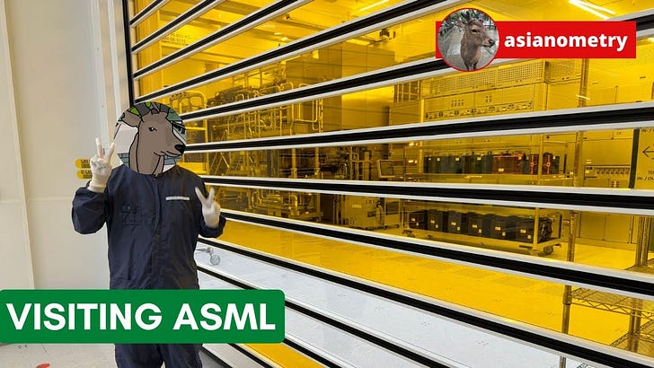
I recently returned from a two week trip to Europe for IMEC’s ITF World 2024. It was a wonderful whirlwind of a journey and had a great time. I received a great deal of ideas for videos and will be working on them over the next few weeks. The trip had many upsides - sorry I didn’t organize any meetups as I was too tired - but the highlight was undoubtedly this trip to ASML.
I recently had the opportunity to visit ASML's headquarters in the small village of Veldhoven in the Netherlands.
It was a wonderful experience. I learned a lot about the company's history, culture, and more.
And I was honored to have the rare opportunity to see the $300 million or whatever High-NA EUV tool. I call it the Beast.
So in this short video, just a few random thoughts on seeing ASML in the flesh.
Eindhoven
My hotel was in Eindhoven, which is short ways near Veldhoven.The town is quite nice, albeit rather slow-paced. By the way. For what it is worth, I paid my own way including transportation and hotel stay. And ASML did not sponsor this video.
Eindhoven will forever be known as the home of Philips, the once-massive consumer electronics tech giant.
They first built the lithography machine technology and later spun off ASML as a joint venture with ASM International.
They were also TSMC's cornerstone foreign investor, owning 28% of the company at the start and 36% later on.
Philips later sold off all the shares they got from both those efforts. As of this writing, the two companies have a combined market capitalization of $1 trillion. Would have been nice to have those stakes now.
But such is life. Investment managers in the mid-1990s were pressuring Philips to sell those stakes to "unlock" shareholder value.
ASML in Veldhoven
Over the past five years, ASML has grown incredibly fast in almost every possible way.For instance, the stock has gone nuts - to the utter surprise of virtually everyone who has ever worked at the company.
The company has gained a huge and unexpected new following in the popular consciousness. That includes a great deal of people who believe that the company's products make chips right out of the box like a pasta machine. Not the case, by the way.
And then headcount. Today the company has over 42,000 employees across Europe, Asia, and the United States. A bit more than half work at the Dutch headquarters.
And some 20,000 of those employees joined the company in just the past five years. That is kind of staggering.
All this past growth - plus anticipated future growth - has caused some issues. For instance, where to put them. The company's current campus sits between two highways, which constrains its growth.
On one side you have natural protected areas that cannot be developed. Not to mention that there is a very large highway in the way.
On the other side you have residential development and homes, which I assume belong to the village of Veldhoven. I don't think it is in the company's best interest to irritate those people by surrounding them with big industrial buildings. So what can you do?
The company wants to expand their factories to add more capacity for EUV and DUV machines, particularly the former. There are also concerns about having enough water and power.
Plus transportation. Most people have to drive in because Veldhoven is a literal village and the roads are not adequate to handle all that. So the company is negotiating with the local governments about that.
Debate
Those negotiations have caused a bit of a ruckus recently.A few stories made it into the news about the company potentially "leaving" the Netherlands. You have stories of something called "Project Beethoven", a $2.5 billion incentives plan by the government to "keep" the company in the Netherlands.
The name is rather dramatic - fit for a movie. But it does no favors to the core issue. To me it seems fair that one of the things that governments should do for their residents, businesses included, is to provide infrastructure.
But the negotiations have stirred up a debate in the government. A group of Dutch people have the sentiment of "Just go then!"
And indeed, several previously dual-headquartered companies like Shell and Unilever have left the Netherlands for the United Kingdom.
But based on what I have seen and heard, I don't think leaving the Netherlands is an option. Veldhoven has been ASML's home since they were unceremoniously dumped there after the Philips spinoff.
So much of the company's supplier base and talents live and work here. ASML is not going to pull an Oracle and force them to relocate. They want to stay. But if there is nowhere to expand, then they seem to be open to doing that expansion elsewhere.
Fortunately, that doesn't seem necessary. In April, the company signed a letter for land for a second campus somewhere north of the Eindhoven airport - close to the current campus.
Culture
Let us talk about company culture.TSMC and ASML are like siblings. They share a corporate parent. TSMC turned to ASML and their lithography machines to defeat the then-dominant Japanese semiconductor makers. And over the next thirty years, they grew up together.
I can feel how their cultures align. Both companies have a strain of “get it done” and "no excuses" culture. They are both very technical. When discussing issues, their focus is almost always on the science and technology. They like geeks and builders.
At ASML, people have to be ready to argue and back their points because their peers will challenge them on it. "Challenge" is one of their core values.
Perhaps it has a bit to do with the Dutch attitude, which is famously blunt.
So the company's recent massive hiring wave presents a big challenge:
How to integrate all that new talent and bring them into ASML's unique culture?
I am reminded of the big hiring sprees that the American tech giants like Google and Meta experienced during the pandemic. With all that new hiring, there inevitably has been some loosening of standards.
Right now, times are good. But as they say in a famous show, "winter is coming".
Early on, ASML lost millions struggling to compete in the stepper market, surviving only thanks to government subsidies. And even later on, the industry's frequent cyclical downturns have meant layoffs.
The company's struggles are engrained in its literal architecture. Their office buildings were designed such that they can be hived off and rented out if necessary.
As the Old Guard luminaries start to retire - like CTO Martin van den Brink, who has been around since the very beginning - I can’t imagine that people aren’t wondering about how to retain the things that made the company successful.
The fate of ASML's old parent company Philips serves as a stark reminder of what can happen if people get complacent and the old culture is lost.
Philips is still around in Eindhoven. The name is everywhere. ASML’s parts labeling number system comes from Philips. When I visited ASML, Philips was then doing a popup shop, selling lights and coffeemakers.
But today Philips is a mere husk of what they used to be - taken down by suffocating bureaucracy and excessive invention.
If you want to learn more about ASML's history and rise, I do again recommend the book "Focus" by Marc Hijink. It is very thorough and on the point.
Competitors
ASML has a monopoly on EUV. I don't think that is changing.The technology cost billions of dollars to produce. A competitor would start 20 years behind. And with the number of buyers so limited, they would never make their R&D investment back.
But most of what ASML ships in a given year are standard DUV TWINSCAN machines. These DUV machines are the industry's workhorse and pattern the vast majority of an integrated circuit - everything but its deepest, densest parts.
The DUV machines do indeed have a lot of competition from the Japanese - Nikon and Canon. Historically, they were the market leaders, and the companies are still around today. They are a formidable crew.
And of course, the Chinese lithography-makers like SMEE are also trying to get there too. They are far behind, but highly motivated.
For this reason, ASML focuses a great deal on productivity and improving cost of ownership. It is the idea behind the TWINSCAN’s twin scan. ASML's goal is not to make the prettiest or even cheapest machine.
Or the machine that most satisfies the armchair semiconductor engineers on Twitter or HackerNews.
ASML's goal is to make a machine that offers the best value for its customers - the most accurate and productive machine possible. Even a billion dollar machine can make sense for the fab if it can accurately do enough wafers per hour.
Building Machines
I was curious to see how they assemble the lithography machines in the cleanrooms. But I probably should not have been so surprised.The cleanroom factory reminds me for some reason of a very bright, very clean Home Depot. It is a bustle of activity with workers in blue or white bunny suits walking about - sometimes with equipment.
By the way. Despite the fact that ASML’s product is a physical thing, it seems like only a minority of its employees work the factory floors. Most work in offices - sales, software, and the such.
Anyway. Down a few hallways, we have these medium sized, well-lit rooms. Inside each room, there is an EUV or DUV system being assembled, like a patient in a hospital room. The machine gets put together using the customer's requested modules, and then tested.
The customer reviews the data and the simulation tests and signs off.
After that, the machine gets pulled apart into modules again over the span of eight to ten days. ASML then carefully ships those parts over to the customer's fab. After the customer gets the machine pieces, another team carefully puts it together over a much longer period of time. They run a final spec check and if that is all good then it's the customer's.
During my visit, ASML was in the midst of assembling some High-NA EUV machines. So I got to see some of those modules first. The easily identifiable modules are the laser, light source, illumination optics, reticle stage, projection optics, and wafer stage.
Very quickly, here is how it works. The drive laser generates EUV light in the light source. The light gets evenly spread out in Illumination. It then bounces off the reticle/mask and gains the chip design information. That light then gets shrunk down in the Projection module before finally hitting the wafer.
The Beast
I was honored to have a chance to see the Beast - a fully-assembled High-NA EUV machine, the EXE:5000.The Beast sits in its own room somewhere within the ASML factory. It is about two stories tall - a massive conglomerate of wires, pipes, tubes, flashing lights, and metal frame. The first thing I said when I saw it was: “this thing is insane!”.
It wasn’t even everything. The drive laser, a massive CO2 laser from the German company Trumpf, sits in a nearby room. Those and other sub-fab components take up two whole floors.
The metal is particularly striking - shiny stainless steel that looks fresh out of the CNC milling machine. Everywhere you look on this thing, you see luminous steel and rough, sharp edges.
When you are in the room with the Beast, you hear pumps constantly whirring - like vacuum cleaners. I am told that you get used to the sound.
The Beast is so large that it has its own ladder and platform attached to it. You can climb up on top of it and look down on the various modules like the light source.
The old Low-NA EUV machine had its light source near the machine's bottom - I guess where you'd call its belly.
The Beast raises its light source up to the end of its spine. This lets them take out one mirror, a big boon since each mirror reduces the EUV light power by 30%. I expect that innovation to eventually filter into the Low-NA EUV machines too.
The machine was extensively re-engineered from Low-NA. Now knowing that the EUV light collector mirrors need to be replaced every so often, the designers rejiggered things to make that mirror easier to access.
The wafer stage is the same as the older machines. But because the mask field size has been cut in half, the reticle stage has been engineered to move twice as fast to overcome that productivity hit.
It moves so insanely fast you cannot believe it is also making movements that are precise to the nanometer.
And the machine's whole top can be lifted up and set down on itself. I like that little design touch. That is done using a custom-built, automatically-guided crane inside the cleanroom. Yes, it needs a crane.
I am not sure if the Beast was running at the time I visited it. But the Belgian research institute IMEC and ASML are working together on a High-NA EUV ecosystem and that includes offering a pilot line with the Beast for potential customers to make test wafers.
And to add, I do think TSMC will eventually buy these machines. Most analysts agree with me here - even the initially skeptical ones. TSMC likes the technology, just not the price.
If that is all there is, then I am sure they will close the gap and bring the Beast to TSMC fab floors.
Hyper
Where are we going next?There is no light wavelength after EUV. You are basically at X-rays now and that stuff is hard to project and manipulate using lens. Optical is everything at ASML. They don’t seem to believe in e-beam direct.
So it is Hyper-NA EUV, then. But does that mean the machine is about to get even larger? In a few years, am I going to be standing in front of an even bigger Beast?
ASML people are aware that that’s not feasible and they talk of ways to keep the size from blowing up again one more time. We shall see what brilliant tricks they can come up with.
It took ASML 10 years to do High-NA EUV. If ASML decides to do Hyper-NA EUV right now and it takes a similar development cycle, then the company - and the industry as a whole - has some form of vague clarity of its lithographic future into at least 2040.
Conclusion
I want to sincerely thank the people at ASML for their kind hosting and thoughtful replies to my idiotic questions.We focus a lot on ASML's machines, but I think there should be more attention on ASML itself - the machine that builds those machines.
The people at ASML are aware that High-NA EUV does not work, right now. There are many problems. There is more than a little skepticism floating around, particularly on the Internet.
But the company has faced similar doubts before. TWINSCAN, 193 nanometer immersion, and EUV all did not work at the beginning too. The first EUV machine took 23 hours to pattern a single wafer. Today’s best EUV machines can do 180 wafers per hour.
The key thing was to get going on it, and to work closely with the fabs and the rest of the semiconductor ecosystem to eventually get there. If there is a pathway to making it work, then that is enough.
To me, that is the sort of technological optimism that we all need to have more of in our lives.
