fansink
Well-known member
Multi-protocol subsystem delivers 8 Tbps/mm bandwidth density and 24 Gbps D2D data rate for hyperscale, HPC, and AI applications
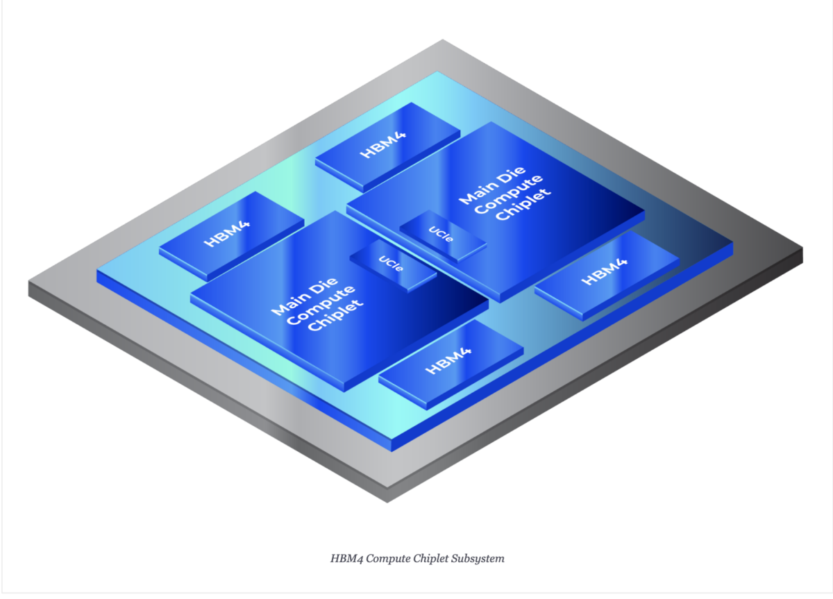
Alphawave Semi (LSE: AWE), a global leader in high-speed connectivity and compute silicon for the world’s technology infrastructure, has unveiled the availability of the industry’s first 3nm silicon-proven Universal Chiplet Interconnect Express (UCIe™) Die-to-Die (D2D) IP subsystem, built on TSMC’s Chip-on-Wafer-on-Substrate (CoWoS®) advanced packaging technology.
“Our recent collaboration with Alphawave Semi exemplifies how we collaborate with our Open Innovation Platform® (OIP) ecosystem partners to enable significant advancements in packaging, meeting the increasing demands in AI and HPC applications,” said Dan Kochpatcharin, Head of Ecosystem and Alliance Management Division at TSMC. “We will continue our partnership with Alphawave Semi to advance the 3D IC design ecosystem to empower faster and power-efficient semiconductor designs.”

Unveiling the Industry’s First Silicon-Proven 3nm, 24Gbps UCIe™ IP Subsystem with TSMC CoWoS® Technology
Alphawave Semi (LSE: AWE), a global leader in high-speed connectivity and compute silicon for the world’s technology infrastructure, has unveiled the
www.businesswire.com

