You are currently viewing SemiWiki as a guest which gives you limited access to the site. To view blog comments and experience other SemiWiki features you must be a registered member. Registration is fast, simple, and absolutely free so please, join our community today!
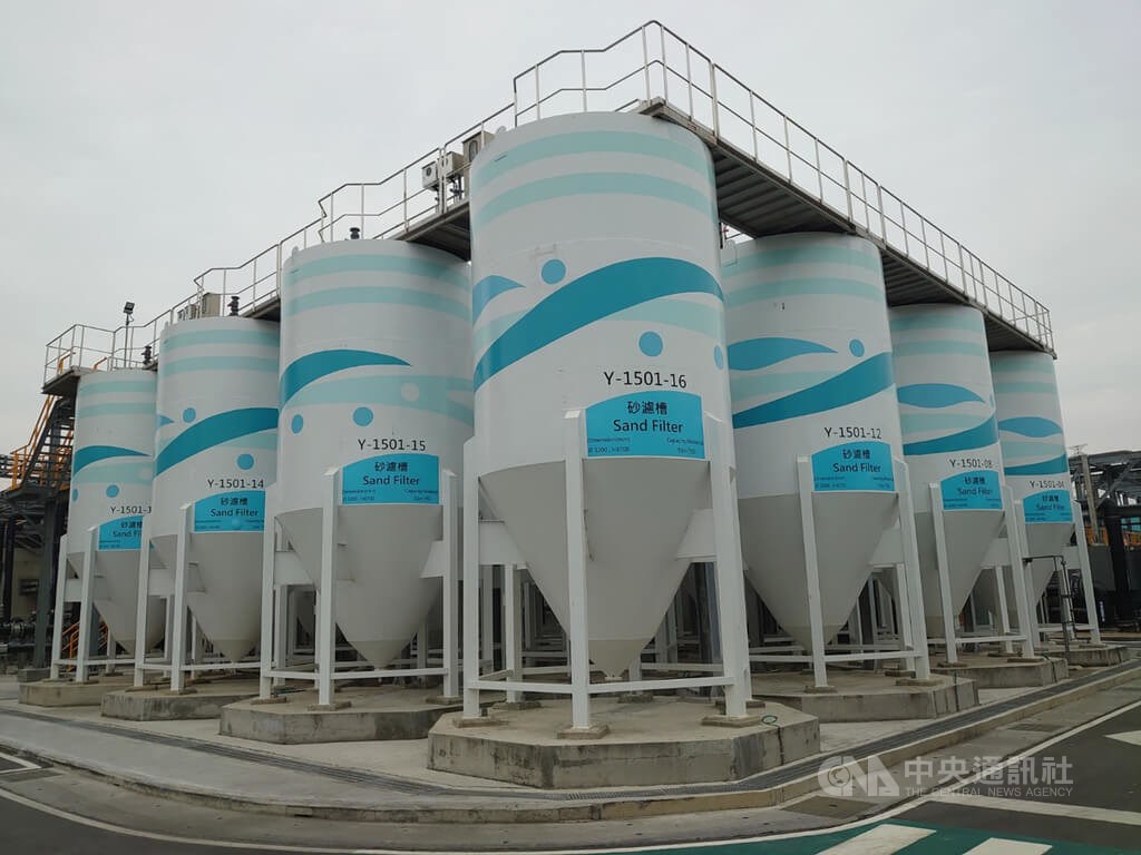
Taiwan Semiconductor Manufacturing Co. (TSMC) on Tuesday reiterated plans for comprehensive water treatment and recycling facilities in Arizona, amid reports the contract chipmaker could fall victim to "water politics" in the drought-affected U.S. state.
focustaiwan.tw
In a statement, TSMC said it planned to construct a water recycling facility to meet the needs of its advanced wafer fabs in Phoenix, adding that it would also build a comprehensive waste-water treatment system to reduce consumption and increase efficiency.
Interestingly, the first fab is no longer targeted for 5nm but 4nm.
TSMC mentioned this at the Symposium. From what I learned TSMC can recycle > 90% of the water used. Same with Intel. But yes, they are building fabs in the desert.
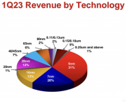
TSMC also mentioned making N4 and N3 wafers. N4 is the same fab as N5 so no big difference there. They did not say which versions of N4 and N3 but my guess would be the HPC versions since AI is the big leading edge driver for future wafer sales.
Not only are TSM and Intel having a conflict over water in Arizona, TSM is having water problems in Taiwan. With the intellectual power that will be brought to solving the water shortage I see water recycling methods and programs going on steroids to not only solve the challenge for fabs, but...
TSMC mentioned this at the Symposium. From what I learned TSMC can recycle > 90% of the water used. Same with Intel. But yes, they are building fabs in the desert.
TSMC also mentioned making N4 and N3 wafers. N4 is the same fab as N5 so no big difference there. They did not say which versions of N4 and N3 but my guess would be the HPC versions since AI is the big leading edge driver for future wafer sales.
Seems like TSMC will be getting huge migration to N3E and it’s derivatives. What is to come of N7 capacity? The current generation of gaming consoles use N7 which must be huge orders but I wonder what TSMC is planning to do with these fabs and capacity once that’s no longer the case. Will this be another N10 situation where it rapidly dies out? Hopefully TSMC can do something to transition the capacity.
Seems like TSMC will be getting huge migration to N3E and it’s derivatives. What is to come of N7 capacity? The current generation of gaming consoles use N7 which must be huge orders but I wonder what TSMC is planning to do with these fabs and capacity once that’s no longer the case. Will this be another N10 situation where it rapidly dies out? Hopefully TSMC can do something to transition the capacity.
Run them to the end of time like they do with almost all of their nodes. To my knowledge the only main nodes that got EOLd was 10FF and 20nm. In both of these cases it was done rapidly after 16FF and N7 came to market. Given TSMC hasn't done this to N7 yet, they built a large amount of capacity for that node family, and that customers/TSMC don't view it as a pitstop node to bigger and better things: N7 will pressubilby be run for the long haul. Also as Dan mentioned they have announced automotive and RF versions of N7 family. This is not behaviour that would be consistent with getting rid of the node anytime over the next decade or two at the bare minimum.
Run them to the end of time like they do with almost all of their nodes. To my knowledge the only main nodes that got EOLd was 10FF and 20nm. In both of these cases it was done rapidly after 16FF and N7 came to market. Given TSMC hasn't done this to N7 yet, they built a large amount of capacity for that node family, and that customers/TSMC don't view it as a pitstop node to better things N7 will pressubilby be run for the long haul. Also as Dan mentioned they have announced automotive and RF versions of N7 family. This is not behaviour that would be consistent with getting rid of the node anytime over the next decade or two at the bare minimum.
Those were Apple specific nodes (20nm and 10nm) and no they were not rapidly EOLd. Apple business has quite a world wide tail to it. TSMC 20nm was the iPhone 6 which was a huge success and continued for years.
Those were Apple specific nodes (20nm and 10nm) and no they were not rapidly EOLd. Apple business has quite a world wide tail to it. TSMC 20nm was the iPhone 6 which was a huge success and continued for years.
Rapidly in the grand scheme of things for foundry operations. Of course by intel standards that was a normal process ramp and de-ramp cycle. As for being "Apple specific nodes" that doesn't seem to be the case. I remember seeing multiple fabless customers talk about how they could design for 20nm but they decided to just wait on 16FF because the PPA advantages over 28nm did not justify the time/design/wafer costs over 28nm when 16FF was such a fast follow. As for 10FF TSMC's website claims the node has the IP to support baseband, mobile, and ASIC designs. Just some quick browsing around also shows multiple mediatek and Huawei SOCs that were built with the node as well as an old Xiaomi chip built on 10FF.
Rapidly in the grand scheme of things for foundry operations. Of course by intel standards that was a normal process ramp and de-ramp cycle. As for being "Apple specific nodes" that doesn't seem to be the case. I remember seeing multiple fabless customers talk about how they could design for 20nm but they decided to just wait on 16FF because the PPA advantages over 28nm did not justify the time/design/wafer costs over 28nm when 16FF was such a fast follow. As for 10FF TSMC's website claims the node has the IP to support baseband, mobile, and ASIC designs. Just some quick browsing around also shows multiple mediatek and Huawei SOCs that were built with the node as well as an old Xiaomi chip built on 10FF.
TSMC also mentioned making N4 and N3 wafers. N4 is the same fab as N5 so no big difference there. They did not say which versions of N4 and N3 but my guess would be the HPC versions since AI is the big leading edge driver for future wafer sales.
TSMC mentioned this at the Symposium. From what I learned TSMC can recycle > 90% of the water used. Same with Intel. But yes, they are building fabs in the desert.
TSMC also mentioned making N4 and N3 wafers. N4 is the same fab as N5 so no big difference there. They did not say which versions of N4 and N3 but my guess would be the HPC versions since AI is the big leading edge driver for future wafer sales.
how is the N5 fab the same as N4? Asking because I have no idea and would like to learn. I was under the assumption that at least some high-end equipment would have to be replaced.
how is the N5 fab the same as N4? Asking because I have no idea and would like to learn. I was under the assumption that at least some high-end equipment would have to be replaced.
N4 is an optimized version of N5. Same as N7 and N6. Same level of EUV etc... You can tell with the TSMC quarterly reports, they only report N16, N7, and N5. All variations in the same fab are not reported separately.
My understanding based on TSMC statements/techinsights teardowns is that it is just a 2% optical shrink (4% density boost) with small performance/variability enhancements. Based on my understanding from Fred's writings EUV is kind of at the point that small upgrades to the tools or process can let you do small shrinks at iso-DD or keeping pitches the same and reaping better DDs. Because it is just an optical shrink DRs will be unchanged allowing for easy "porting".
 focustaiwan.tw