You are currently viewing SemiWiki as a guest which gives you limited access to the site. To view blog comments and experience other SemiWiki features you must be a registered member. Registration is fast, simple, and absolutely free so please, join our community today!
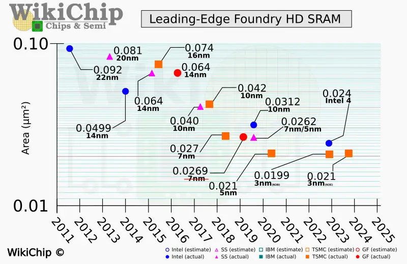
IEDM 2022: Did we just witness the death of SRAM? While foundries continue to show strong logic transistor scaling, SRAM scaling has completely collapsed.
fuse.wikichip.org
Chip area scaling expected to be limited now by SRAM, particularly those chips emphasizing AI.
Surely everyone saw this coming right? This is a key reason why chiplets are such a good idea. Offload SRAM which has been scaling horribly for years now. Can even use a cheaper process on the SRAM. Monolithic dies are an endangered species (my opinion).
Surely everyone saw this coming right? This is a key reason why chiplets are such a good idea. Offload SRAM which has been scaling horribly for years now. Can even use a cheaper process on the SRAM. Monolithic dies are an endangered species (my opinion).
IEDM 2022: Did we just witness the death of SRAM? While foundries continue to show strong logic transistor scaling, SRAM scaling has completely collapsed.
fuse.wikichip.org
View attachment 986
Chip area scaling expected to be limited now by SRAM, particularly those chips emphasizing AI.
I found this plot very odd. Samsung was still on a linear curve at 7/5nm. I wonder if their 5nm sram scaled by a similar amount to their logic. I wonder what they've been doing to be getting more consistent sram scaling. Is it because 7nm had aggressive M0 pitches compared to N7? I would love to see 3GAE sram density and how it compares to N5 given they should be much closer in density than 5nm and N5. Presumably as SS rolls out nodes that catch up to intel and TSMC current/near future offerings on density they must hit the same scaling walls as the rest, but in the meantime good job SS for keeping up at 10/7nm sram race.
Any idea what they will use? I have heard next to nothing about N2 GAA implementation, I am more concerned about how logic is scaling. Is N2 logic scaling poorly just because it is yield learning, or should be concerned about what comes after N2?
Any idea what they will use? I have heard next to nothing about N2 GAA implementation, I am more concerned about how logic is scaling. Is N2 logic scaling poorly just because it is yield learning, or should be concerned about what comes after N2?
If N2 is a small or 0 density improvement I wouldn't be that broken up or scared. N3's issues might cause a delay to N-1, which is more concerning. I would have to assume more density will come with it, but don't expect an N7 sized jump (IMO we will never see anything as big as that from TSMC ever again without multiple stacks of logic becoming a thing). By the time of N-1 or N-2 high NA will likely be starting to roll out, and that will make further lithographic shrinks feasible (still up in the air if metals and channels can keep up) at the cost of max reticil size. Presumably BPR/BSPD CFET and the like will give SRAM a couple of shots in the arm. HNS probably less so given HD SRAM often has very few fins.
If N2 is a small or 0 density improvement I wouldn't be that broken up or scared. N3's issues might cause a delay to N-1, which is more concerning. I would have to assume more density will come with it, but don't expect an N7 sized jump (IMO we will never see anything as big as that from TSMC ever again without multiple stacks of logic becoming a thing). By the time of N-1 or N-2 high NA will likely be starting to roll out, and that will make further lithographic shrinks feasible (still up in the air if metals and channels can keep up) at the cost of max reticil size. Presumably BPR/BSPD CFET and the like will give SRAM a couple of shots in the arm. HNS probably less so given HD SRAM often has very few fins.
What gives extra shock value is the scaling rate slowed down as more EUV added, pitches shrunk, although gate pitch also scaled slower (new architectures don't seem to help much either).
What gives extra shock value is the scaling rate slowed down as more EUV added, pitches shrunk, although gate pitch also scaled slower (new architectures don't seem to help much either).
Is TSMC known to sandbag performance? They usually do for the financial performance of the business. But yeah I am rather surprised by how anemic the density “improvements” are for N2. It is shocking
Is TSMC known to sandbag performance? They usually do for the financial performance of the business. But yeah I am rather surprised by how anemic the density “improvements” are for N2. It is shocking
If N5 and N3 are anything to go off of; no. It seems TSMC over exaggerated N5's density and they very publicly failed to hit N3 density or performance targets.
As for N2 being a small bump it is expected. N16 is no denser than it's predecessors (BEOL was unchanged). This is a deliberate move to increase cadence and roadmap reliability. If N2 was a big jump I would be genuinely worried for TSMC, but they are playing it safe (which I and their customers like). Slow and steady wins the race.
Zen 4's IPC is actually better than what AMD originally saidAMD formally launched the Ryzen 7000 (with availability four weeks away though) and confirmed specs and pricing. The company has also disclosed a considerable amount of technical details and more has now leaked from unofficial sources...
Zen 4's IPC is actually better than what AMD originally saidAMD formally launched the Ryzen 7000 (with availability four weeks away though) and confirmed specs and pricing. The company has also disclosed a considerable amount of technical details and more has now leaked from unofficial sources...
I was speculating that perhaps moving it off die might be feasible considering that Zen4 L2 cache latency is already high, and presumably accepted enough by their customers, that further increases in latency might also be acceptable.
Otherwise moving it off die wouldn't be feasible. I was asking if anyone knew what that increase could look like.
L2 I could never imagine because of how it is split between specific cores. L3 is much more feasible. But I would love to hear the opinion of any CPU designers.
I didn't know this was a thing. Man Pentium had alot of weird packaged variants to boost it's competitiveness (Pentium-D springs to mind). Would I be right to assume this scheme wouldn't work with modern L2 caches in multi-core processors given L2's tight integration with individual cores?
I didn't know this was a thing. Man Pentium had alot of weird packaged variants to boost it's competitiveness (Pentium-D springs to mind). Would I be right to assume this scheme wouldn't work with modern L2 caches in multi-core processors given L2's tight integration with individual cores?