Thank you Ian for your feedback. You brought up many good points that I found valuable.
For the others...
 www.imec-int.com
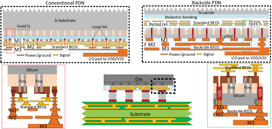
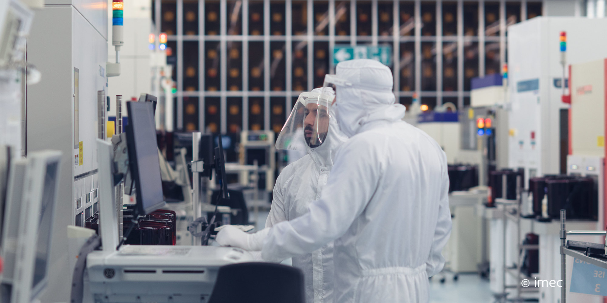
For the first time, imec has evaluated the impact of backside wafer thinning and n-TSV fabrication on the characteristics of scaled Si-channel FinFET test devices (gate length ≥20nm), built in the wafer’s frontside. The backside connectivity was realized through tungsten-filled n-TSVs that land on metal-1 pads in the wafer’s frontside. Naoto Horiguchi, director CMOS device technology at imec: “The most important conclusion of this work is that wafer thinning and n-TSV processing in the backside did not show any negative impact on the performance of the FinFETs, except for a slight degradation of the pMOS drive current. For nMOS, an even higher mobility and drivability (up to 15%) were found after backside processing, and no bias temperature instability (BTI) degradation was observed. In this work, wafers were thinned down to final Si thicknesses ranging between 20 and 370nm.” More details are included in the 2021 VLSI paper by A. Veloso et al. [VLSI-1]
=============================================
Imec must have done this expensive exercise for a reason, and their results appear to be encouraging. In 2025, the ASML CEO predicts 660 DUV machines vs 90 EUV machines will be produced. DUV double patterned processes seem to be more practical for ASICs.
As somebody who 1) Creates stdcells, P&R tools, analyzes EM and voltage drop on supplies, etc, and 2) helps customers with ASICs on DUV processes, I believe the benefits of the backside supply connections through the bottom of the substrate is huge.
Are there any other predictions out there by process people of the viability of GF, TSMC-Japan, and Intel doing this on their 12nm + processes?
For the others...
Imec demonstrates critical building blocks for a backside power delivery network | imec
In several papers presented at the 2021 Symposia on VLSI Technology and Circuits (VLSI 2021), imec reports progress in developing enabling technologies for a backside power delivery network. First, the impact of backside wafer processing on the performance of ‘frontside’ FinFET devices was...
For the first time, imec has evaluated the impact of backside wafer thinning and n-TSV fabrication on the characteristics of scaled Si-channel FinFET test devices (gate length ≥20nm), built in the wafer’s frontside. The backside connectivity was realized through tungsten-filled n-TSVs that land on metal-1 pads in the wafer’s frontside. Naoto Horiguchi, director CMOS device technology at imec: “The most important conclusion of this work is that wafer thinning and n-TSV processing in the backside did not show any negative impact on the performance of the FinFETs, except for a slight degradation of the pMOS drive current. For nMOS, an even higher mobility and drivability (up to 15%) were found after backside processing, and no bias temperature instability (BTI) degradation was observed. In this work, wafers were thinned down to final Si thicknesses ranging between 20 and 370nm.” More details are included in the 2021 VLSI paper by A. Veloso et al. [VLSI-1]
=============================================
Imec must have done this expensive exercise for a reason, and their results appear to be encouraging. In 2025, the ASML CEO predicts 660 DUV machines vs 90 EUV machines will be produced. DUV double patterned processes seem to be more practical for ASICs.
As somebody who 1) Creates stdcells, P&R tools, analyzes EM and voltage drop on supplies, etc, and 2) helps customers with ASICs on DUV processes, I believe the benefits of the backside supply connections through the bottom of the substrate is huge.
Are there any other predictions out there by process people of the viability of GF, TSMC-Japan, and Intel doing this on their 12nm + processes?