Scotten Jones
Moderator
I took that same course at IEDM, I also know Paul pretty well. With all due respect to Paul, a few comments.just for the context:
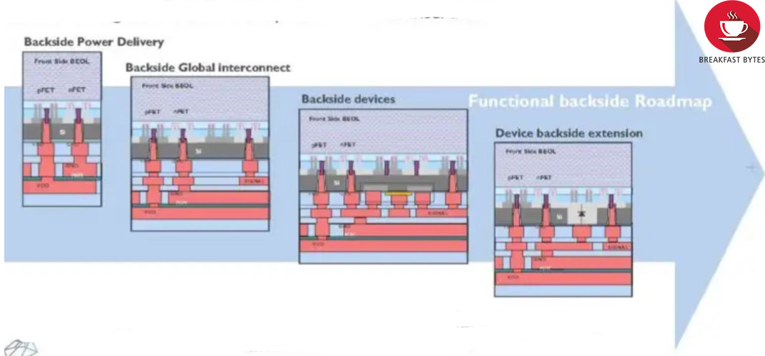
IEDM: Backside Power Delivery
<a href="https://community.cadence.com/cadence_blogs_8/b/breakfast-bytes"></a>One part of the short course that I attended at IEDM in December was about backside power delivery networks. It was presented by Gaspard Hiblot of imec and titled Process Architectures Changes to Improve Power...community.cadence.com
"As I'm sure you have heard, simple dimensional scaling (aka Moore's Law) is running out of steam, and DTCO approaches are required to keep scaling on track."
What Gordon Moore originally said was "The complexity for minimum component costs has increased at a rate of roughly a factor of two per year (see graph on next page)."
I don't know why people keep saying certain scaling techniques don't qualify as Moore's law, in my view DTCO is just another method of extending Moore's law. I have also seen people exclude 3D NAND from Moore's law because it is in the third dimension. Moore's law is slowing but as long as cost per transistor or cost per bit is going down, whatever method is used to achieve it is still "Moore's law".
The reason copper resistivity increases at small dimensions is electron scattering, copper has a relatively long electron mean free path. Ruthenium with a shorter electron mean free path doesn't have the resistivity increase at small dimensions as fast as copper and at small enough dimensions has a lower resistivity than copper, even though copper has a lower bulk resistivity. Scattering does occur at surfaces and grain boundaries but it is electron scattering that is the ultimate driver. At small dimensions the figure of merit for a conductor is electron mean free path multiplied by bulk resistivity. By this measure Rhodium is the best metal known but it is so difficult to work with that Ruthenium (second best) is the long term metal of choice.
Currently no one is using Ruthenium as an interconnect layer although it is used as a seed for copper plating due to the superior resulting copper properties. Cobalt was used by Intel as interconnect at 10nm/7nm and cobalt has been used for contacts but multiple companies, but the latest processes have moved away from cobalt.
He shows a figure showing 300 ohm via chain resistance, an interesting data point on this from IEDM is TSMC showed for their 3nm process the via chain resistance is actually ~560 ohms, making an even stronger case for Backside Power Delivery (BPD).
With respect to buried power rails (BPR), in a nutshell you take wide-thin power rails from metal 2 and replace them with tall-narrow rails embedded in the substrate. This allows for closer cell to cell placement. This is an interesting technology but my understanding is none of the major logic producers want to put metal in the wafer before fabricating the transistors. For their 20A process in 2024 Intel will be the first to introduce BPD (PowerVia), Samsung and TSMC have both announced backside power delivery for second generation 2nm processes around 2026. Intel is not using BPR, I am not sure but I don't think TSMC is either, I don't know what Samsung is doing. My Imec contact agrees BPR won't be used for first generation BPD but believes it will eventually be needed.
There are varying views on the need for BPR, Imec believes BPD with BPR is denser than Intel PowerVia, but in Applied Materials presentations they show PowerVia as denser. I have discussed this with Imec and they say Applied Material is using the wrong connection scheme for BPR. Everyone does appear to agree direct backside contact is the most dense solution but is difficult to implement. I asked a contact at ASML about backside alignment, I remember many years ago there were special aligners that looked at the back and front of the wafer simultaneously, my contact said the wafers are so thin for BPD they can just align through the wafer.