Never forget physics.
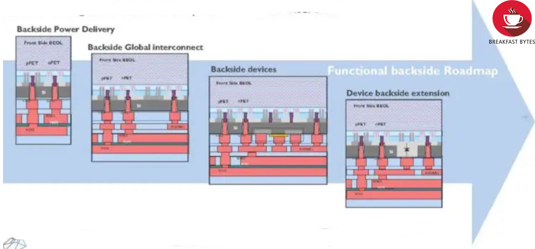
In CMOS you want a well behaved switch and this impose a lot of constraints for electrostatics. When you look at nanowires/sheets, regardless of their orientation in space, you have some critical dimensions you cannot ignore so there are limits (lower and upper) for the thickness of such layers. If you stay on the horizontal plane for your channels, you choose the best thickness of the wire/sheet for electrostatic control and adapt the x/y dimensions for other optimisations. And if you need more current you just superimpose more wires/sheets without loss of density. Source and drain are coplanar and you can access them and have them fully symmetrical, same for the gates. If you go vertical, as before the electrostatic impose the diameter of the wire but now it also fixes your W as it is the circumference of the wire. If you need more current you need wore wires and you lose surface density. You are re-introducing the link between W and the area taken by the device as it was between finfet. You get away with that for VNAND as you can do with lousy transistors, the design is a highly regular structure and the pitches are relatively large, but logic is another beast and you need more than just SRAM even if it is a dominant part of the design. In the examples above you have that all the transistor in the same column have the same W, that is a big restriction for design, just consider matching p and n currents.
Moreover, vertical channels are not symmetric as the extension you will need for S/D contacts on top or bottom will have different geometries as you can see from some of the previous figures. And schemes like those sometimes looks more as a show-off of mastering Coventor than a real process flow with an associated reticle set.
Do not forget routing: anywhere one of those local interconnects needs to get to a metal line for distribution you cannot put transistors on top so you have an extra density loss.
3D is certainly the way forward but is not easy and not all challenges are solved, one of those is place and route in real 3D and not 2.5D. Another is the capability of having good epi growth on very small areas and then propagating it vertically. Some of the monolithic 3D demonstrations have been either on very large structures or using bonding of crystalline layers on top of insulators. And keeping the strain that gives you the carrier mobility in some of those structures will also be challenging.
They should merge IEDM and ISSCC and have more plenary sessions so that device/process/circuit people talks more to each other ....