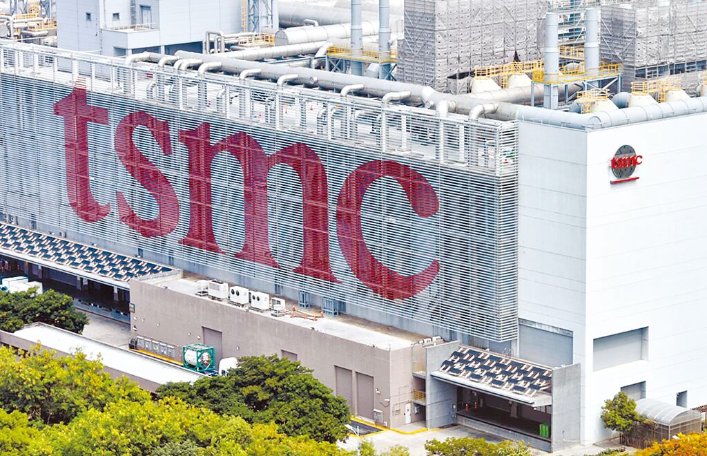
TSMC's Baoshan plant is expected to install capacity in April and compete with the Kaohsiung plant for mass production in 2025; it will compete with Intel, Samsung, etc.

It is pointed out that TSMC will accelerate the production of 2nm in April, not only to gain time for advanced process yield ramp-up, but also to continue to pose a threat to Samsung and Intel and open up their lead. Picture/Photo from this newspaper's data
The demand for AI is strong, and there are reports from the semiconductor supply chain that TSMC's Hsinchu Baoshan Fab20 P1 plant will carry out equipment installation work in April to warm up for mass production of the GAA (gate-all-around) architecture. Baoshan P1 and P2 are expected and Kaohsiung's three advanced process wafer fabs will all enter mass production in 2025, and have attracted customers such as Apple, Huida, AMD and Qualcomm to compete for production capacity.
TSMC did not express any opinion on this rumor.
Semiconductor industry players say that whether the wafer manufacturing industry can make a lot of money depends on the yield rate after mass production of the process. The key lies in the yield ramp-up speed. The longer it takes, the higher the cost. Although Samsung claims to be the first to develop the GAA architecture before overtaking in corners, It is said that the yield rate is not good enough to open up the market.
It is pointed out that TSMC's 2nm will accelerate its machine entry in April, not only to gain time for advanced process yield ramp-up, but also to continue to pose a threat to Samsung and Intel and open up their lead. The supply chain revealed that TSMC has prepared for the installation of P1, which is expected to be trial production in the fourth quarter and mass production in the second quarter of next year. Equipment manufacturers pointed out that they have recently deployed manpower and conducted education and training in advance to meet TSMC's customized needs.
As a new milestone in the chip manufacturing process, 2nm will provide higher performance and lower power consumption; adopt nanosheet technology structure, and also develop backside power rail technology. TSMC believes that 2nm will continue TSMC's technology leadership and capture AI growth business opportunities.
The cost of 2nm chips is very high. Research institutions pointed out that compared with 3nm, the cost will increase by 50%, and the single cost of each wafer will climb to US$30,000; therefore, the first batch of adopters will still be smartphone chips. Customer—Apple.
Different from 3nm, the complex design requires customers to start developing products with TSMC earlier. The market speculates that many customers such as MediaTek, Qualcomm, AMD and Huida have already cooperated; TSMC's press conference also emphasized that the number of N2 customers More than N3 at the same development time.
The competition in 2nm development is fierce. ASML plans to produce 10 2nm EUV lithography machines this year, of which Intel has ordered 6 units. Rapidus Semiconductor Manufacturer, established in Japan with a nationwide effort, is also targeting the 2nm process.
