Array
(
    [content] => 
    [params] => Array
        (
            [0] => /forum/index.php?threads/nvidia-reportedly-delays-its-next-ai-chip-due-to-a-design-flaw.20725/
        )

    [addOns] => Array
        (
            [DL6/MLTP] => 13
            [Hampel/TimeZoneDebug] => 1000070
            [SV/ChangePostDate] => 2010200
            [SemiWiki/Newsletter] => 1000010
            [SemiWiki/WPMenu] => 1000010
            [SemiWiki/XPressExtend] => 1000010
            [ThemeHouse/XLink] => 1000970
            [ThemeHouse/XPress] => 1010570
            [XF] => 2021370
            [XFI] => 1050270
        )

    [wordpress] => /var/www/html
)

Nvidia reportedly delays its next AI chip due to a design flaw

Daniel Nenni

Admin
Staff member
acastro_180529_1777_nvidia_0002.0.jpg

Illustration by Alex Castro / The Verge

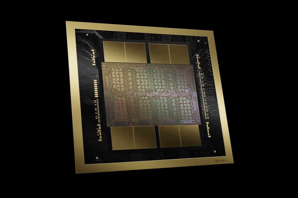
Nvidia has reportedly told Microsoft and at least one other cloud provider that its “Blackwell” B200 AI chips will take at least three months longer to produce than was planned, according to The Information. The delay is the result of a design flaw discovered “unusually late in the production process,” according to two unnamed sources, including a Microsoft employee, cited by the outlet.

B200 chips are the follow-up to the supremely popular and hard-to-get H100 chips that power vast swaths of the artificial intelligence cloud landscape (and helped make Nvidia one of the most valuable companies in the world). Nvidia expects production of the chip “to ramp in 2H,” according to a statement that Nvidia spokesperson John Rizzo shared with The Verge. “Beyond that, we don’t comment on rumors.”

Nvidia is now reportedly working through a fresh set of test runs with chip producer Taiwan Semiconductor Manufacturing Company, and won’t ship large numbers of Blackwell chips until the first quarter. The Information writes that Microsoft, Google, and Meta, have ordered “tens of billions of dollars” worth of the chips.

The report comes just months after Nvidia said that “Blackwell-based products will be available from partners” starting in 2024. The new chips are supposed to kick off a new yearly cadence of AI chips from the company as several other tech firms, such as AMD, work to spin up their own AI chip competitors.

 
Does anyone know the real story here? Design flaw? This could open the door for competitors, absolutely. I will ask around at the FMS conference next week. Then comes Hot Chips and the the GF Summit.
 
Three months late does not sound like a big deal. The only companies with competitive GPU parts are AMD and Intel, and I wonder... even if these two can get the extra chips, can they get them packaged? And then, can the customers' software run on anything but Nvidia GPUs without modifications, and will the software ports take more time to resolve than waiting three extra months?
 
Three months late does not sound like a big deal. The only companies with competitive GPU parts are AMD and Intel, and I wonder... even if these two can get the extra chips, can they get them packaged? And then, can the customers' software run on anything but Nvidia GPUs without modifications, and will the software ports take more time to resolve than waiting three extra months?
Yeah that’s basically redo do some schematics, redo the layout and spin some layers.
 
Does anyone know the real story here? Design flaw? This could open the door for competitors, absolutely. I will ask around at the FMS conference next week. Then comes Hot Chips and the the GF Summit.
New news stories, stemming from a SemiAnalysis report, are pointing to teething pains with CoWoS-L

“The main issue behind these delays to GPU shipments is related to Nvidia's physical design of the Blackwell family, according to a report from semiconductor research firm SemiAnalysis. Specifically, Blackwell is the first high volume design to use the CoWoS-L packaging technology from TSMC, Nvidia's chip manufacturer.”


Didn't expect that silicon interconnects(Intel's term: EMIB) to be this difficult. Maybe it's also the reason why Intel Sapphire rapids(uses 6 silicon bridges) suffered so much.
 
Didn't realize the SemiAnalysis article was available. Fascinating to read about the whole stack of Blackwell server HW challenges from chip-level interconnect, to network interconnect (NVLink), to thermal and power management for the racks. A few things jump out at me - TSMC CoWoS-L looks a lot like Intel EMIB, silicon interposer (CoWoS-S) has hit its reticle limits with the MI300, and with all the rack-level thermal and interconnect issues, perhaps Cerebras has gotten things right for the high end of AI with wafer scale integration.

 
Didn't expect that silicon interconnects(Intel's term: EMIB) to be this difficult. Maybe it's also the reason why Intel Sapphire rapids(uses 6 silicon bridges) suffered so much.
FWIW just remember these are already extremely complex devices. EMIB and packaging just adds more complexity. They’ll master this stuff eventually.
 
They’ll master this stuff eventually.
It might not be master-able with CoWoS-L, Intel EMIB or CoWoS-S (silicon interposer) approaches, once AI complexity forces the substrate sizes to the Blackwell and MI300 scale. Based on this video, Blackwell might be just “too big” for a composite substrate with different CTEs. And AMD is at the reticle limit for silicon interposers. Intel is using EMIB, but seems to be moving to glass substrates for their larger systems. And Cerebras seems to have made the brave jump to wafer scale, resolving all the issues that have killed off prior wafer scale companies. But their approach also requires tradeoffs - greater homogeneity of dies, required redundancy techniques, and a single process (optimized for logic, not memory, today).

 
Last edited:
That Cerebras whiteboard session is a fantastic explanation of the packaging complexities.

You mention glass substrates. I tried to search online but couldn’t find an answer: do glass substrates help fix the CTE mismatch issue with Silicon?

I wonder if this type of issue is what drove Intel to announce their aggressive productionization timeline to ramp up the glass substrate ecosystem?
 
You mention glass substrates. I tried to search online but couldn’t find an answer: do glass substrates help fix the CTE mismatch issue with Silicon?
I had to look - most glasses (Silicon Dioxide) are closer in CTE to silicon, which helps reduce the mismatch. The video pegs the silicon CTE at 2.6 ppm / K, and organic substrates at 10 ppm/K.

 
That Cerebras whiteboard session is a fantastic explanation of the packaging complexities.
No one has more respect for what Cerebras has accomplished than I do, and the video is awesome, but the Cerebras solution of wafer-scale chips are not for everyone. Take a look at the CS-3 16RU rack chassis. 23KW, is rumored to cost about $2M (the actual price is not published), and, I don't know for sure, but I suspect you can't just plop an H100 workload on it without what I guess is essentially application redevelopment.

Take a peek at this monster. I like the way they position it at about the size of a dorm room fridge. Yeah, right. A $2M, 23KW dorm room mini-fridge. I love it.

 
Last edited:
the Cerebras solution of wafer-scale chips are not for everyone.
I kind of thought the same thing until I read the SemiAnalysis article - that woke me up to the systems/rack issues NVIDIA and its partners are dealing with. The CS-3 is roughly comparable to a full refrigerator-sized NVL-32 Blackwell rack. If I read the article right an NVL-32 MGX rack uses a little less than 2x the power of a CS-3 and requires about 4x the space (the doubled power of the NVL-32 MGX forces typical data centers to have to leave alternating empty racks for sufficient air cooling). Seems like there might be a sweet spot for AI Data Centers.


You're right on the software though. But I think NVIDIA's moat lies in a different place than most people think. The leading LLMs that we hear about so much are all written in standard AI frameworks like PyTorch, so fairly easy to port models to different AI processors, though optimization requires smarts by each AI "engine" supplier. I think NVIDIA has differentiated themselves by the sophisticated enterprise-level app development system on top of the models - all the stuff that that they rolled out at the last GTC. Cerebras is at the stage where they can ramp up new customer applications leveraging essentially services and learn how to generalize from each customer. I think that AMD has learned that the battle has moved to the Gen AI applications level, which inspired them to buy Silo.ai (GenAI services company). NVIDIA has gone the Gen AI enterprise application platform and ecosystem approach instead of the services approach.
 
For anyone interested (a deep knowledge of computer architecture helps), this is Cerebras's WSE-2 architecture presentation. It's very well done, but, like I said, it can easily whoosh over the heads of those who can't think "oh yeah, that's cool" when the author starts discussing BLAS levels. :) (I have the same problem with many of @Fred Chen posts. I hear a lot of whooshing, and resort to internet searches for clues.)

 
You're right on the software though. But I think NVIDIA's moat lies in a different place than most people think. The leading LLMs that we hear about so much are all written in standard AI frameworks like PyTorch, so fairly easy to port models to different AI processors, though optimization requires smarts by each AI "engine" supplier. I think NVIDIA has differentiated themselves by the sophisticated enterprise-level app development system on top of the models - all the stuff that that they rolled out at the last GTC. Cerebras is at the stage where they can ramp up new customer applications leveraging essentially services and learn how to generalize from each customer. I think that AMD has learned that the battle has moved to the Gen AI applications level, which inspired them to buy Silo.ai (GenAI services company). NVIDIA has gone the Gen AI enterprise application platform and ecosystem approach instead of the services approach.
Cerebras does support PyTorch according to their website, and they describe how to port a trained model to Hugging Face, but I haven't seen any testimonials from groups that have transitioned successfully to Cerebras system from a GPU-based system. Yet.
 
Back
Top