jms_embedded
Well-known member
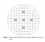
I've noticed on some photographs of wafers that some of the dice are different. For example:
https://pixels.com/featured/odomete...its-adam-hart-davisscience-photo-library.html -- 5 different dice near top/middle/bottom
https://www.computerhistory.org/revolution/digital-logic/12/288/1639 -- 5 dice are different, forming a cross (one in center, one near top/left/bottom/right)
https://compote.slate.com/images/df4dfbfe-9846-4c86-a168-aeed9608704e.jpeg -- 1 die in each 6x4 grid
What are these called and what are they for? (process quality control?)