Understanding the hurdles in advancing AI technologies, from energy consumption and memory demands to interconnect limitations and scalability for next-generation systems
Source: TSMC
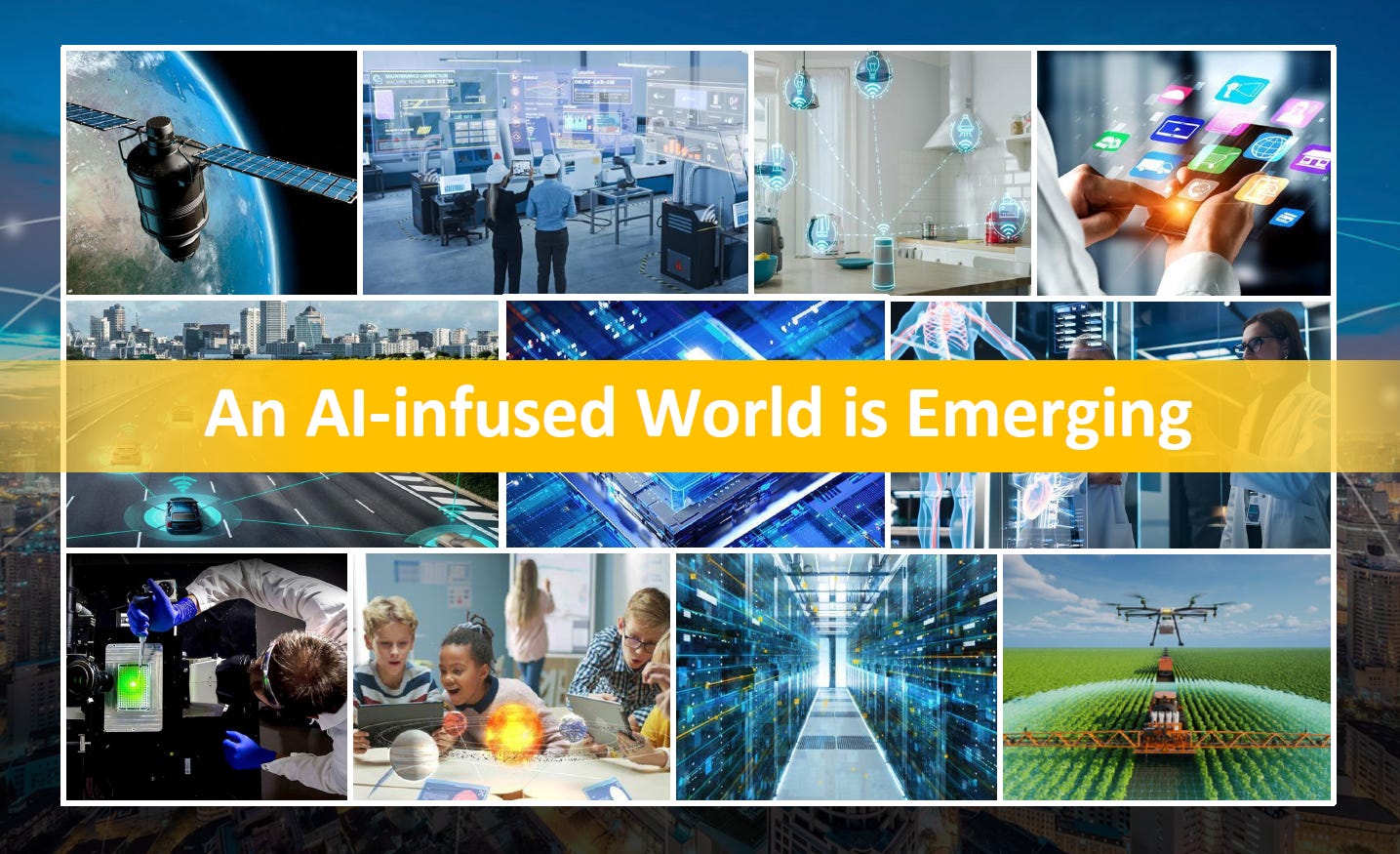
An AI-infused world is rapidly emerging, transforming industries and daily life. From advanced space exploration and smart cities to personalized healthcare and precision agriculture, AI is revolutionizing how we interact with technology. It enables breakthroughs in education, energy efficiency, and autonomous transportation, showcasing its potential to address global challenges.
With AI seamlessly integrated into various sectors, the future promises enhanced innovation, productivity, and connectivity, shaping a smarter, more sustainable world.
Challenges Faced by AI Systems
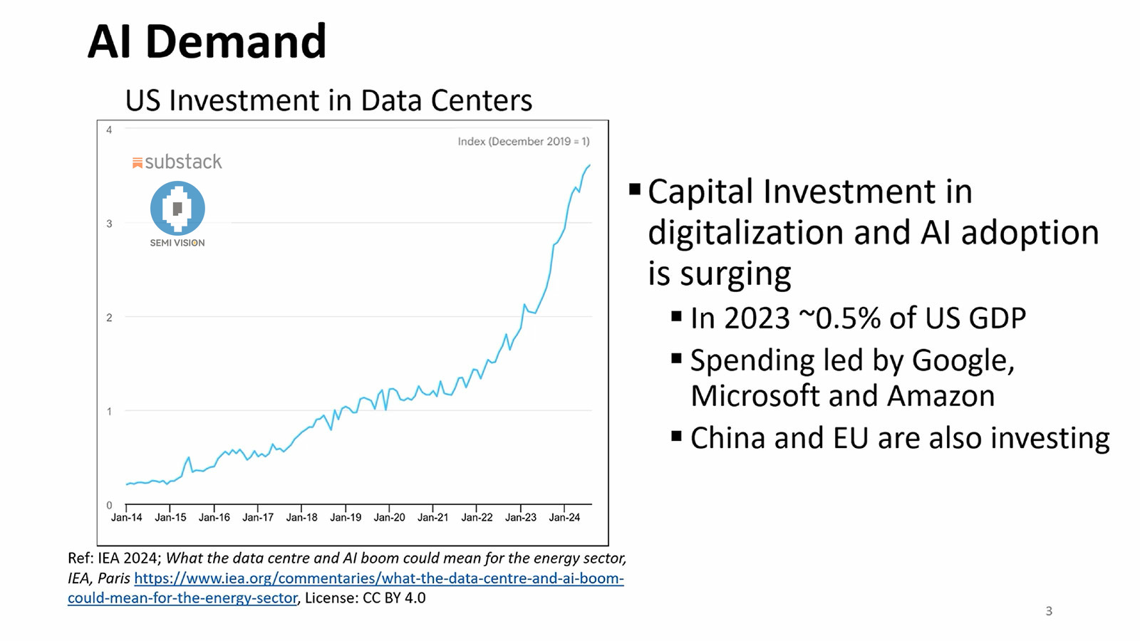
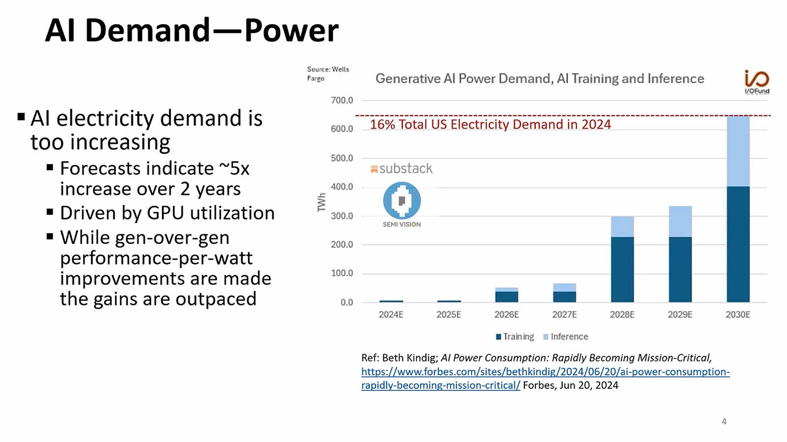
1) Massive Power Consumption Issue
Source: IEDM
According to the rapid growth of AI-related electricity demand since 2014, driven by the widespread deployment of AI systems. This surge is primarily fueled by GPU utilization for both AI training and inference tasks. Projections indicate that AI systems could consume up to 16% of total U.S. electricity by 2030—a startling estimate. Over just two years, electricity demand for AI is expected to increase 5x. Although advancements in GPU performance-per-watt are being made, these gains are not enough to offset the growing energy consumption caused by the expanding scale of AI systems.
Source: IEDM
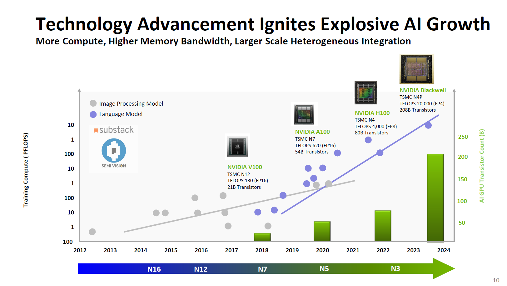
These GPUs significantly increase training compute power, measured in PFLOPS, to meet the demands of AI workloads, including image processing and large language models. The sharp jump in performance, especially between 2027 and 2028, aligns with the mass production of advanced nodes like 2nm and beyond. This growth is supported by higher memory bandwidth and larger-scale heterogeneous integration, ensuring more compute power for AI's expanding needs.
Source: TSMC
Interestingly, while most power consumption is currently dominated by AI training, inference tasks are expected to grow significantly as large language models (LLMs) require substantial energy for processing. Managing this exponential demand will necessitate significant innovations in energy efficiency and hardware optimization. Modular architectures, improved interconnects, and energy-efficient AI chips will be critical, alongside adopting renewable energy sources and optimizing data center power usage to mitigate environmental impacts. As AI-driven workloads increasingly shift focus from training to inference, further escalating electricity demand, balancing performance and sustainability will be essential to ensure the scalability and long-term viability of AI technologies.
Enhancing Chip Design with LLM
2) Memory Issues
Source: IEDM
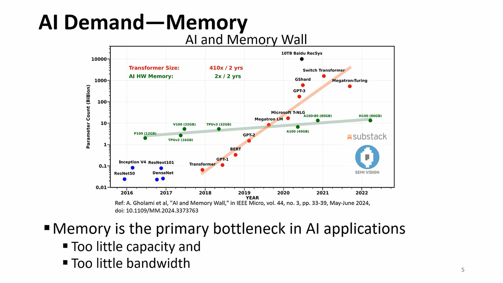
Another critical issue is memory. While memory capacity is doubling every two years, LLMs are expanding at an unprecedented pace, with network sizes growing 410 times every two years. This has led to a dual shortage in memory capacity and bandwidth.
AI boom still running hot as SK Hynix says its already sold majority of its 2025 allotment of high-bandwidth memory chips
Source: blocksandfiles.com
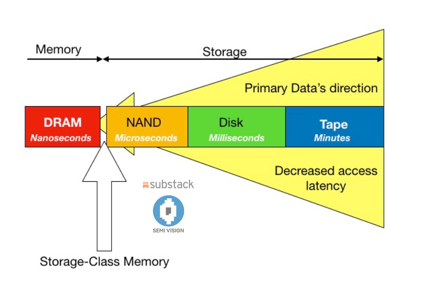
While Storage Class Memory (SCM) could address capacity issues, these memories are far too slow to keep up with computational speeds, leading to bottlenecks. Thus, both memory capacity and bandwidth must improve simultaneously.
Source: semiengineering.com
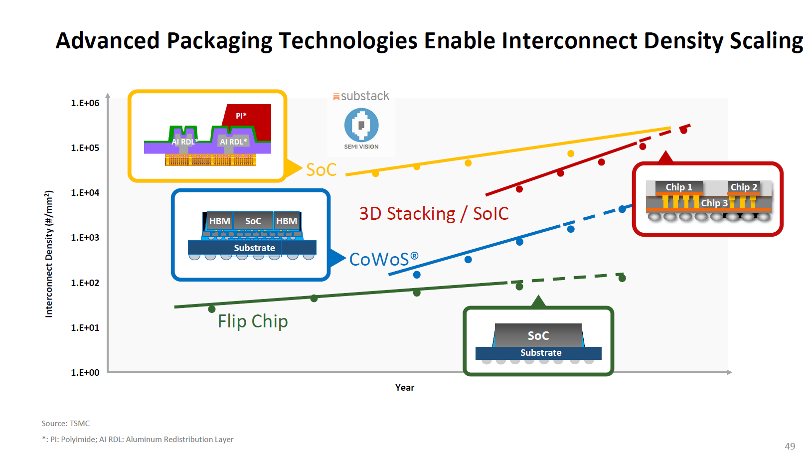
HBM and Advanced Packaging Lead the Way
Source: TSMC
3) Interconnect Limitations
Interconnect limitations play a crucial role in driving AI chips toward advanced packaging because traditional interconnect technologies cannot meet the growing demands of AI workloads.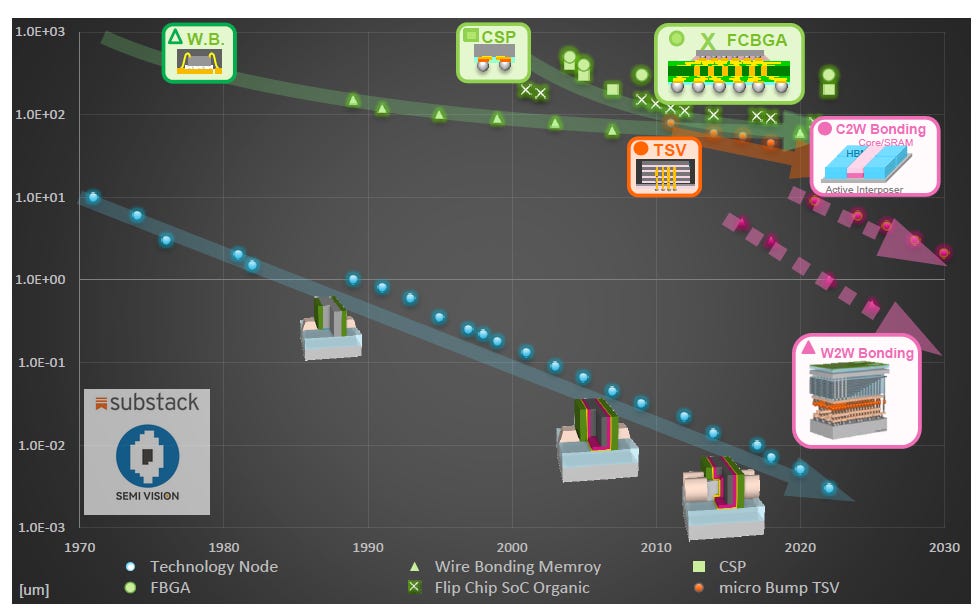
Source: TEL
- Wire Bonding, used primarily in older technologies, gradually reduces in size over time.
- CSP (Chip Scale Packaging)and FBGA (Fine-pitch Ball Grid Array) are modern packaging methods for smaller nodes, particularly relevant for mobile and consumer applications.
- FCBGA (Flip Chip Ball Grid Array) and TSV (Through-Silicon Via) represent more advanced packaging, integrating multi-die stacks, typically used in high-performance applications.
- C2W Bonding (Chip to Wafer) , W2W Bonding (Wafer to Wafer) , and micro Bump TSV represent newer packaging approaches, focused on 3D integration and smaller node sizes, offering enhanced interconnectivity and performance.
Source: TSMC
AI chips require extremely high data transfer rates and low latency to handle massive amounts of data, especially in training and inference tasks for large models like LLMs. However, conventional interconnects face challenges such as:
- Bandwidth Bottlenecks: Traditional interconnects struggle to provide sufficient bandwidth for high-performance AI systems, leading to delays and inefficiencies in data movement between processing units.
- Energy Efficiency: Energy consumption increases significantly with larger-scale interconnects, making it impractical for systems to scale using traditional methods without advanced power-saving solutions.
- Integration Challenges: Modern AI systems often require multiple chips or modules to work together seamlessly, which demands tighter integration than traditional interconnects can offer.
- Scaling Constraints: As AI models grow in size, the need for compact, high-density interconnects to integrate chiplets and memory components becomes critical.
4) Advanced Packaging and Interconnect Solutions
UCIe (Universal Chiplet Interconnect Express) is an industry consortium that develops and promotes a standardized interconnect specification for chiplets. Its goal is to enable seamless communication between chiplets from different vendors, fostering interoperability and modularity in semiconductor design. By establishing a common standard, UCIe aims to enhance the scalability, efficiency, and flexibility of advanced semiconductor systems, facilitating innovation in areas such as AI, HPC, and data centers.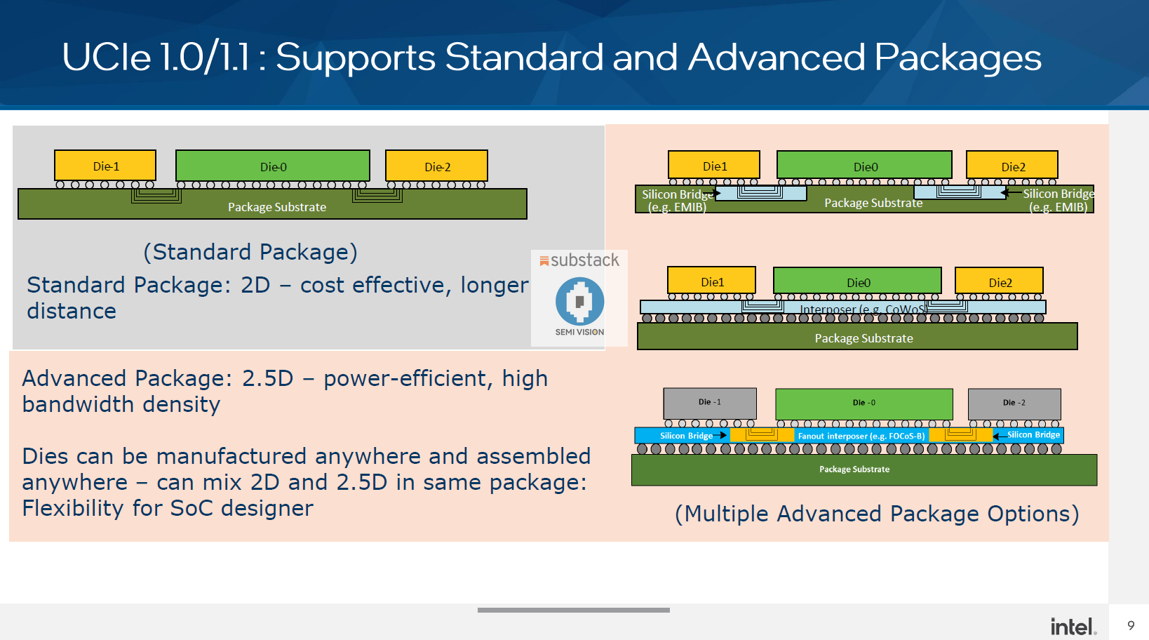
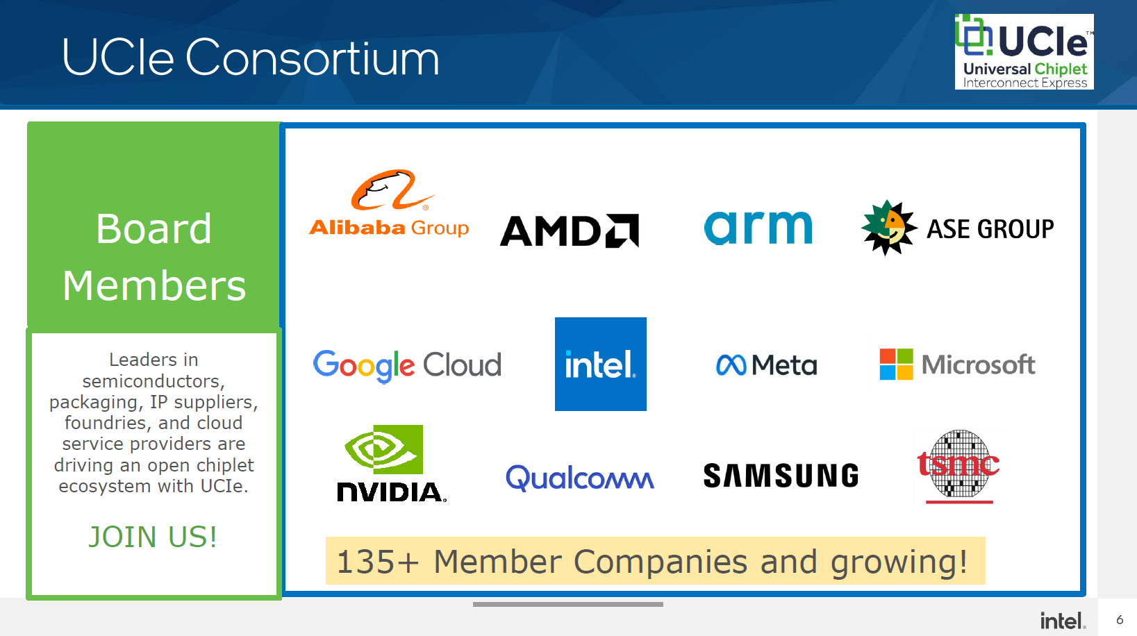
Major companies in the semiconductor industry, including Intel, AMD, TSMC, ARM, ASE and others, are part of this initiative.
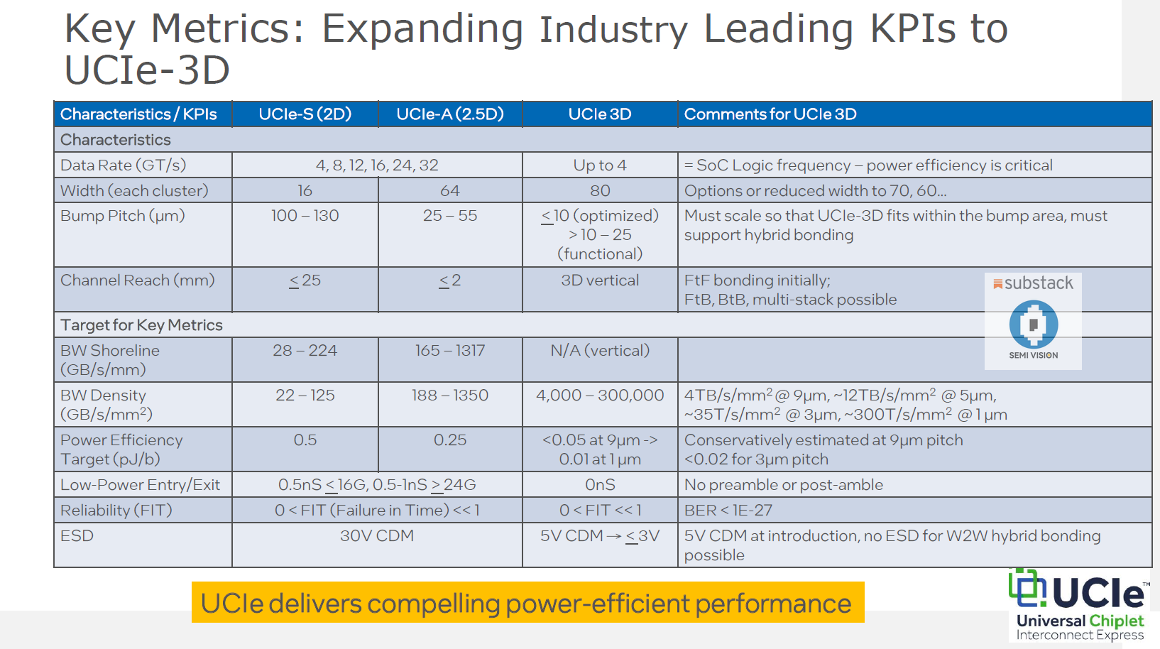
The future of UCIe lies in its ability to expand industry-leading KPIs to UCIe-3D, enabling significant advancements in chiplet interconnect technology. The evolution from UCIe-S (2D) and UCIe-A (2.5D) to UCIe-3D highlights improvements in critical metrics such as data rate, power efficiency, and bandwidth density.
SEMI VISION is a reader-supported publication. To receive new posts and support my work, consider becoming a free or paid subscriber.
Upgrade to paid