
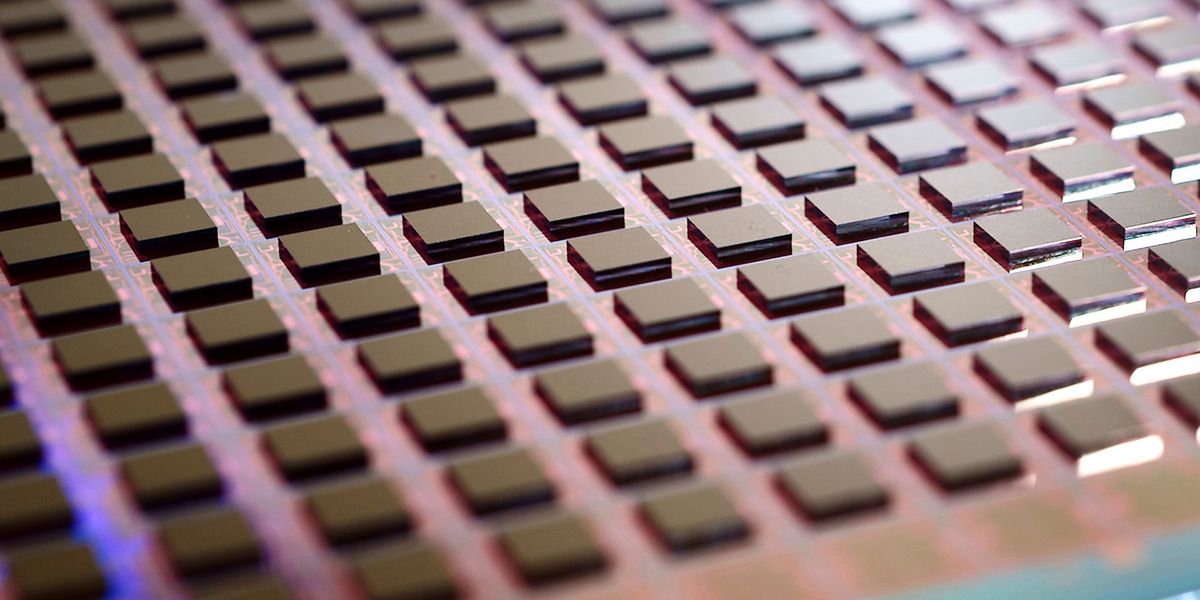
Three-D integration is just one of a number of techniques that will be essential to the future of CMOS—or, as some in the industry are beginning to call it, CMOS 2.0.
IMEC
3D INTEGRATIONMOORE'S LAWSYSTEM TECHNOLOGY COOPTIMIZATIONBACK-SIDE POWER DELIVERYNANOSHEET TRANSISTORSMICROCHIPS
There was a time, decades really, when all it took to make a better computer chip were smaller transistors and narrower interconnects. That time’s long gone now, and although transistors will continue to get a bit smaller, simply making them so is no longer the point. The only way to keep up the exponential pace of computing now is a scheme called system technology co-optimization, or STCO, argued researchers at ITF World 2023 last week in Antwerp, Belgium. It’s the ability to break chips up into their functional components, use the optimal transistor and interconnect technology for each function, and stitch them back together to create a lower-power, better-functioning whole.
“This leads us to a new paradigm for CMOS,” says Imec R&D manager Marie Garcia Bardon. CMOS 2.0, as the Belgium-based nanotech research organization is calling it, is a complicated vision. But it may be the most practical way forward, and parts of it are already evident in today’s most advanced chips.
How we got here
In a sense, the semiconductor industry was spoiled by the decades prior to about 2005, says Julien Ryckaert, R&D vice president at Imec. During that time, chemists and device physicists were able to regularly produce a smaller, lower-power, faster transistor that could be used for every function on a chip and that would lead to a steady increase in computing capability. But the wheels began to come off that scheme not long thereafter. Device specialists could come up with excellent new transistors, but those transistors weren’t making better, smaller circuits, such as the SRAM memory and standard logic cells that make up the bulk of CPUs. In response, chipmakers began to break down the barriers between standard cell design and transistor development. Called design technology co-optimization, or DTCO, the new scheme led to devices designed specifically to make better standard cells and memory.But DTCO isn’t enough to keep computing going. The limits of physics and economic realities conspired to put barriers in the path to progressing with a one-size-fits-all transistor. For example, physical limits have prevented CMOS operating voltages from decreasing below about 0.7 volts, slowing down progress in power consumption, explains Anabela Veloso, principal engineer at Imec. Moving to multicore processors helped ameliorate that issue for a time. Meanwhile, input-output limits meant it became more and more necessary to integrate the functions of multiple chips onto the processor. So in addition to a system-on-chip (SoC) having multiple instances of processor cores, they also integrate network, memory, and often specialized signal-processing cores. Not only do these cores and functions have different power and other needs, they also can’t be made smaller at the same rate. Even the CPU’s cache memory, SRAM, isn’t scaling down as quickly as the processor’s logic.
Keeping Moore’s Law Going is Getting Complicated
CMOS 2.0 will require exceptional creativity to rewire and 3D-stack the chip
 spectrum.ieee.org