You are currently viewing SemiWiki as a guest which gives you limited access to the site. To view blog comments and experience other SemiWiki features you must be a registered member. Registration is fast, simple, and absolutely free so please, join our community today!
2 years ago when Intel announced their "Five nodes in four years," there were a lot of non-believers they were able to achieve it. Now halfway down the road, while we can all have different opinions on what qualifies as a success for Intel, can we agree they are making some good progress in achieving the goal.
My question is:
1. The general expection of a development of a node is at least 2-3 years, yet Intel is progressing so fast they are on one node and simultaneously developing another. It's not like they are just "copying off" TSMC or Samsung, Intel has their own unique package and set of designs. Is this them declaring hey we have all these capabilities and are just demonstrating what they have developed in a short burst one after the other (they may have most of them developed in the past few years, but had some blunders along the way.)
2. Is it the funding Intel has that makes it possible? Their extensive IP library, manufacture experiences and packages? If we were to give SMIC or GF or even IBM the same, will they be able to recreate this feat.
There is probably no simple explanation to this without a deeo overview of the history and technology, but any feedback will be appreciated.
Semiconductor at the bleeding edge truly is incredible, and I'm glad to be here witnessing it all unfold.
It does appear they are on track both technically and on the schedule (from following the comments here of people who clearly know far more about this than I ever will). Can't comment on other factors like cost/yield or viability as a foundry today.
Perhaps this should not be surprising, for two reasons.
Firstly, the process delays at Intel were surely only in a very few of the many, many aspects of the advancing technologies needed and there was almost certainly a backlog of new stuff piling up where progress had not slipped so much.
Secondly, "process node" has now been redefined almost to mean whatever you want it to - much as process geometry is now a fluid marketing term. Intel seems to make a habit of not using industry standard terminology and rebranding everything as unique as if only they do it. It's not really "five nodes in four years" as most of us would see it. But a significant achievement nonetheless.
On the funding question, I would assume this was largely done off existing funding before any of the current subsidies kicked in (indeed have they yet ?). Intel's certainly invested a massive amount over the last decade and I'd guess more than enough to fund this.
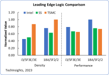
I think there's been quite a lot of commentary on this to the effect that 18A is higher performance but with lower density and likely higher power. That's likely intentional as Intel's chips generally push performance over cost and power. Perhaps Intel could produce something area competitive with TSMC at this node if they had prioritised that ? But perhaps they don't need to.
2 years ago when Intel announced their "Five nodes in four years," there were a lot of non-believers they were able to achieve it. Now halfway down the road, while we can all have different opinions on what qualifies as a success for Intel, can we agree they are making some good progress in achieving the goal.
My question is:
1. The general expection of a development of a node is at least 2-3 years, yet Intel is progressing so fast they are on one node and simultaneously developing another. It's not like they are just "copying off" TSMC or Samsung, Intel has their own unique package and set of designs. Is this them declaring hey we have all these capabilities and are just demonstrating what they have developed in a short burst one after the other (they may have most of them developed in the past few years, but had some blunders along the way.)
2. Is it the funding Intel has that makes it possible? Their extensive IP library, manufacture experiences and packages? If we were to give SMIC or GF or even IBM the same, will they be able to recreate this feat.
If you listen to intel; they will tell you their success is derived from their new module development model, cooperation with vendors, and delivering an annual cadence of consistent improvements. Based on what we can all see it is too early to have an opinion on exactly how impressive things are given we don't know what i3, 20A, and 18A look like yet. Once we do know, then we can have a more nuanced discussion. Looking at things like intel 4 + powervia and the consistently meaty performance kickers, I would preliminary give a good grade.
It would be interesting to see how their development model compares and differs to TSMC/Samsung. TSMC had/has these meaty nodes with small performance kickers every year that by the time the next full node comes out generally closed the gap on performance but in N3's case roughly matched. CC guides that post N3 cost per FET improvements are taking a back seat to delivering a higher total value of ownership vs the prior nodes, so maybe we can expect meatier halfnodes? Or maybe it just means that even as cost decreases slow the power and performance improvements won't? Either way I'm excited to see what they are cooking up. Then you have Samsung who I guess is attempting to have a new node every 4ish years (5 years and counting until we see a real SF3 product and no indication if SF2 or SF1.4 are derivatives of SF3 or not). To make up for the long gap Samsung has the very interesting practice of heavily pimping out their node over time. Over the course of 7LPP's life they added SDB, then contact near active area, followed by COAG, single fin libraries, and some small yet substantial pitch scaling. Even before that they had 14LPP > 11LPP (14 FEOL with 10 BEOL) and 10LPP > 8LPP (heavily pitch and DTCO scaled).
Having the performance (or density) isn't enough, that's not what lead to Intel's 10nm debacle -- it was yield and reliability problems getting the process into production, either because of too small a process window (pushing the rules too hard -- even TSMC have hit this (e.g. in N3, hence only Apple got to use this and everyone else gets N3E) but nothing like as badly as Intel did) or finding reliability/yield problems with new materials/structures (e.g. cobalt interconnect). The most risky things are fundamentally new structures/process flows like PowerVia/BSPD where there can be unforeseen issues, which is presumably why TSMC are waiting till N2 Gen2 instead of introducing it at the start.
Maybe Intel have learned from this, or maybe they'll repeat the mistake of trying to do too many new things all at the same time to try and pass TSMC. There's no way to know until the process is -- or isn't -- in high-volume high-yield mass production...