(Image credit: Intel)
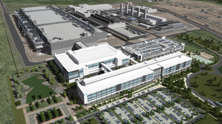
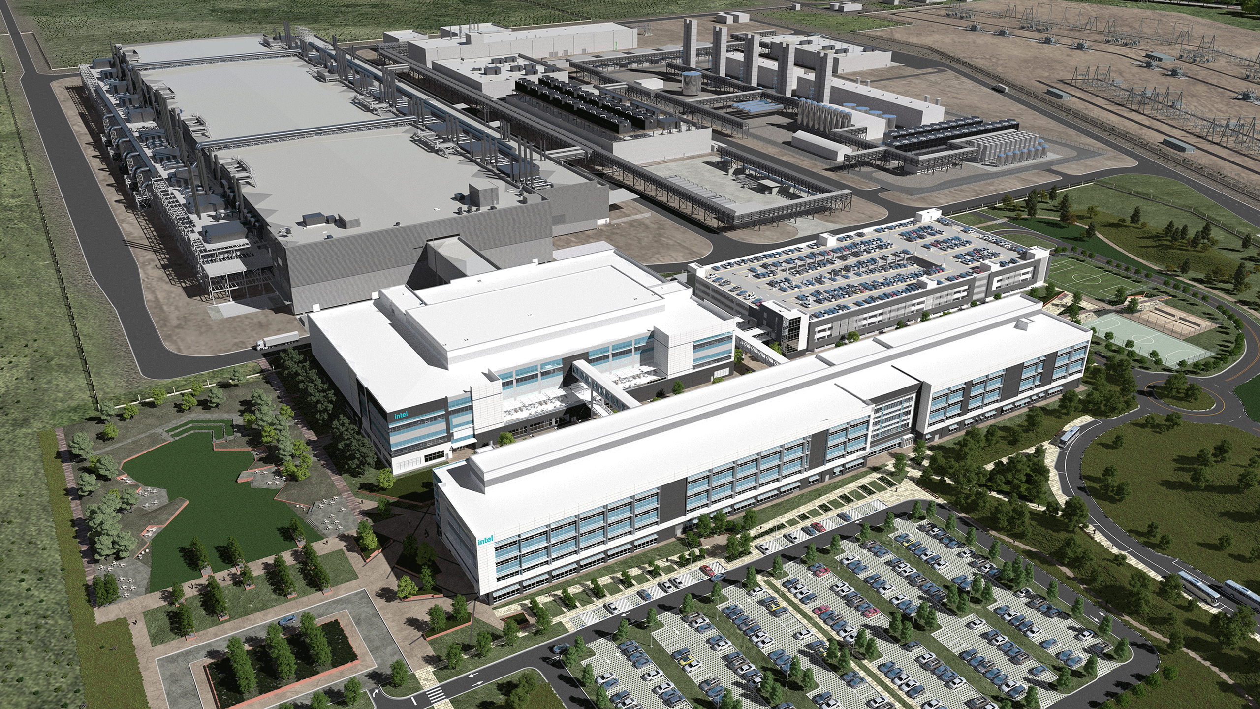
Intel has published detailed plans for its multi-billion site near Magdeburg, Germany that will house two fabs initially and will be able to host up to six additional modules in the future. The plans discovered by HardwareLuxx and Heise.de reveal two large three-story buildings that will accommodate some of the world's most advanced wafer fab tools and will produce some of the most sophisticated chips ever designed. The fabs are now projected to come online in late 2027, which points to very particular process technologies — Intel's 14A (1.4nm) and 10A (1nm) process nodes are certainly on the menu.
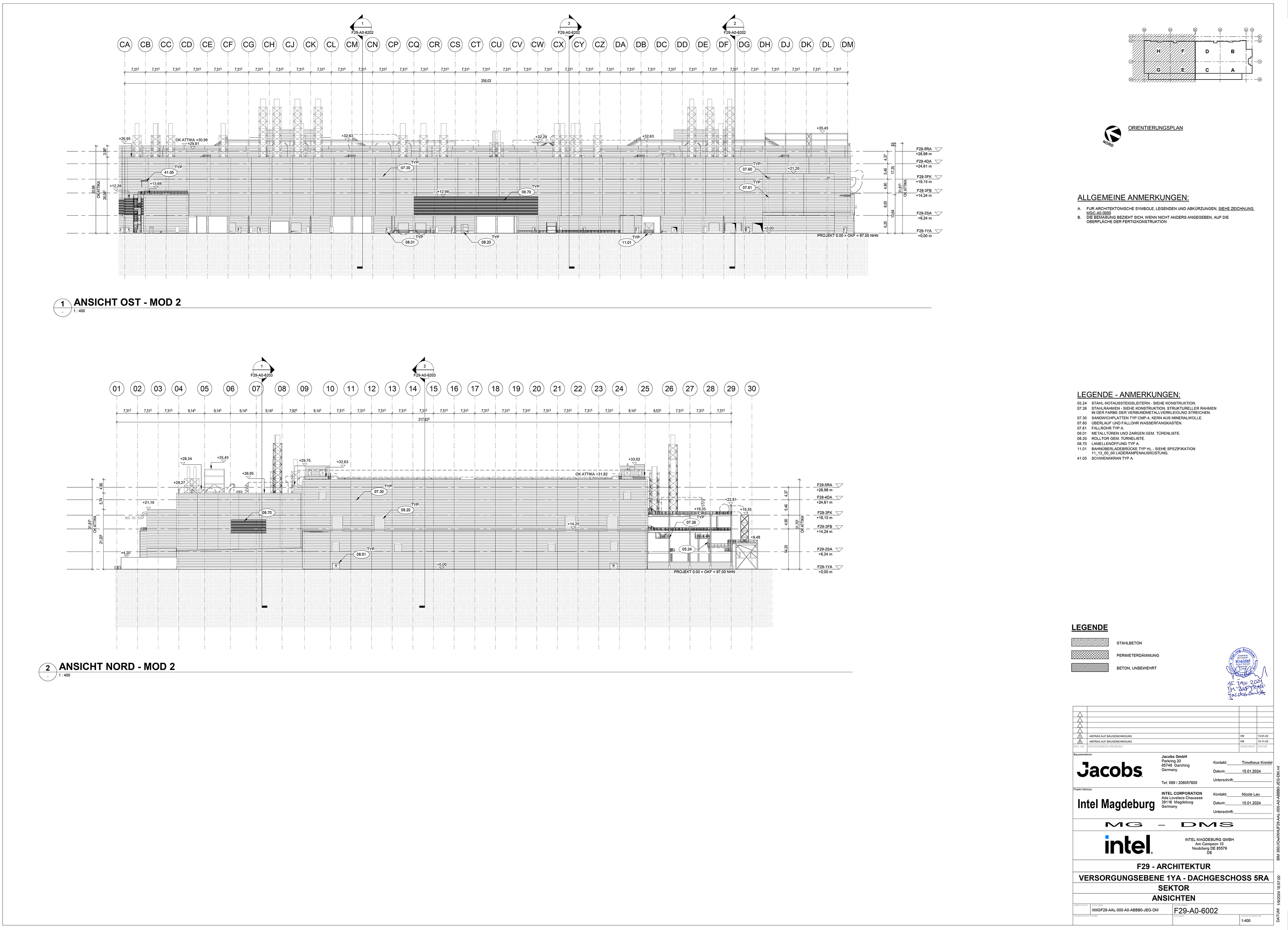
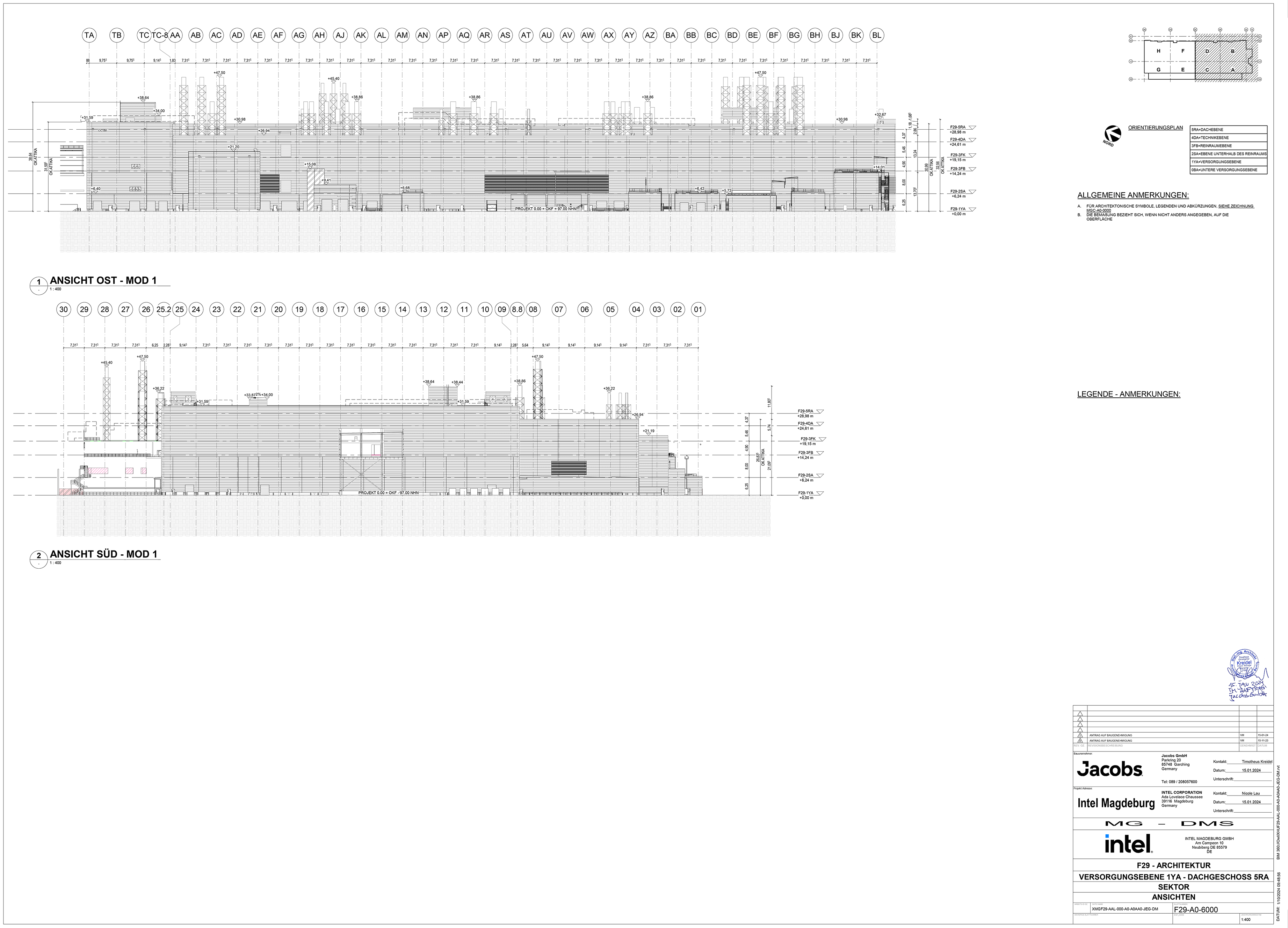
The two modules, Fab 29.1 and Fab 29.2, will cover an area of approximately 81,000 square meters, with a combined length of 530 meters and a width of 153 meters. The buildings, including roof structures for air conditioning and heating, will reach a height of 36.7 meters, but there will be several underground floors, too. The cross-section plans of the fabs above the ground reveal several floors above the ground with heights ranging from 5.7 meters to 6.5 meters.
The second level, with a height of 6.5 meters, will host wafer fab equipment, including Low-NA and High-NA extreme ultraviolet (EUV) lithography tools. The other floors will be dedicated to supplying essential resources such as water, power, and chemicals to the machines.
(Image credit: Intel)
The advanced fab tools will certainly be needed in substantial quantities. Fab 29 is said to be coming online in Q4 2027, so the production facility will be capable of producing chips on Intel 14A (1st gen High-NA-enabled process tech for Intel) and perhaps Intel 10A (2nd gen High-NA process tech for Intel) process technologies.
Image 1 of 2

(Image credit: Intel)

(Image credit: Intel)
ASML models that 1st generation High-NA-enabled production node will use 4 – 9 High-NA EUV exposures and 20 – 30 EUV exposures in total (including Low-NA and High-NA). Given that Intel builds fairly large fabs, one can try and model how many EUV tools it is going to need to process a sizeable number of 14A and 10A wafers.
The site plan for the Intel Magdeburg project shows two modules — Fab 29.1 and Fab 29.2 — alongside numerous support buildings, including cooler and boiling builders (BC1), warehouse (WH1), ultrapure water storage (PB1), special gases storage (BG1), air separation plant (AU1), office building (OB1), service building (SB1), datacenter (DC1), wastewater pretreatment building (WT1), alkaline wastewater pretreatment (NH4W), and parking (PK1).
(Image credit: Intel)
Fab 29 will be connected to the 380-kV high-voltage line that runs there via its own substation. Interestingly, Intel plans to use a battery storage system instead of traditional diesel generators for emergency power, which emphasizes its commitment to sustainability. The newly built road where Intel's Fab 29 will be located is to be named Ada Lovelace Chaussee after the famous physicist and computing pioneer, who happens to also be the namesake for Nvidia's existing gaming GPU architecture.

Intel submits schematics for chip fabs in Germany, two new fabs open in 2027
Detailed plans for two big fabs revealed.
