Array
(
    [content] => 
    [params] => Array
        (
            [0] => /forum/index.php?threads/intel-foundry-update-from-the-investor-call.20722/
        )

    [addOns] => Array
        (
            [DL6/MLTP] => 13
            [Hampel/TimeZoneDebug] => 1000070
            [SV/ChangePostDate] => 2010200
            [SemiWiki/Newsletter] => 1000010
            [SemiWiki/WPMenu] => 1000010
            [SemiWiki/XPressExtend] => 1000010
            [ThemeHouse/XLink] => 1000970
            [ThemeHouse/XPress] => 1010570
            [XF] => 2021370
            [XFI] => 1050270
        )

    [wordpress] => /var/www/html
)

Intel Foundry Update from the Investor Call

Daniel Nenni

Admin
Staff member
The last question was what I was looking for:

Intel Foundry.jpg


Matthew Ramsay
Yes, I do. Thanks, John. I wanted to ask -- I think in some of the prepared script and maybe early in the Q&A, Pat, you kind of reiterated the $15 billion funnel for the Foundry business, and I know in the medium term, a lot of that is packaging, but I wanted to ask about the customers that you've engaged with on 18A and maybe early on 14A, how have you seen the charts of the programs that they're planning to bring into your foundry progress in the last few quarters. Are people still committed to ramping those things? Are they taking PDKs and maybe doing tape-ins? Are things moving forward? Have you seen any acceleration? Have you seen hesitation or maybe wait-and-see from those customers? I'm just trying to figure out how that stuff is progressing on 18A? Thanks.

Patrick Gelsinger
Yes. Let me just clarify, the $15 billion is lifetime deal value of committed deals, right? So this isn't a pipeline. This is committed business that we now have in place. So I just want to clarify that, Matt, because I think your question suggests that the pipeline. There's a lot more in the pipeline. This is $15 billion of committed deals. As you say, a lot of the near-term opportunity has been advanced packaging and we're seeing a significant expansion of that capability in terms of volume and technology. On 18A specifically, a lot of customers have been waiting for the PDK, right, and now that we released the PDK last month, the 1.0 PDK, we've seen a flurry of activity with the EDA, the IP vendors, and the end customers.

So I'd be optimistic that we have good indicators coming in that area in the future, but this was really the starting point for many of them to go from test chips to start looking at production chips coming based on the PDK that we've just released. So we remain very comfortable with our earlier comments in that area. I'd say, we do believe that we'll have further updates there, but as we've also indicated, customers are reluctant to put their name out there given the supply base and the traditional operation of the Foundry industry. Overall, things are looking on track for what we've said with a meaningful acceleration in packaging over the last quarter, more updates to come.

 
Last edited:
Patrick Gelsinger
On 18A specifically, a lot of customers have been waiting for the PDK, right, and now that we released the PDK last month, the 1.0 PDK, we've seen a flurry of activity with the EDA, the IP vendors, and the end customers.
This sound no real order.
 
This sound no real order.

PDKs are a solid signal of customer demand. Generally the big customers start evaluating with PDK .5 for design work. If they trust the PDK they can start designing and as long as there are not big changes from PDK .5 to PDK 1.0 then all is well. Big customers do not wait until PDK 1.0 because of time to market pressures. TSMC's PDKs are trustworthy, Samsung's PDKs are not. Hopefully Intel's PDKs will follow TSMC's lead.
 
The last question was what I was looking for:

View attachment 2152

Matthew Ramsay
Yes, I do. Thanks, John. I wanted to ask -- I think in some of the prepared script and maybe early in the Q&A, Pat, you kind of reiterated the $15 billion funnel for the Foundry business, and I know in the medium term, a lot of that is packaging, but I wanted to ask about the customers that you've engaged with on 18A and maybe early on 14A, how have you seen the charts of the programs that they're planning to bring into your foundry progress in the last few quarters. Are people still committed to ramping those things? Are they taking PDKs and maybe doing tape-ins? Are things moving forward? Have you seen any acceleration? Have you seen hesitation or maybe wait-and-see from those customers? I'm just trying to figure out how that stuff is progressing on 18A? Thanks.

Patrick Gelsinger
Yes. Let me just clarify, the $15 billion is lifetime deal value of committed deals, right? So this isn't a pipeline. This is committed business that we now have in place. So I just want to clarify that, Matt, because I think your question suggests that the pipeline. There's a lot more in the pipeline. This is $15 billion of committed deals. As you say, a lot of the near-term opportunity has been advanced packaging and we're seeing a significant expansion of that capability in terms of volume and technology. On 18A specifically, a lot of customers have been waiting for the PDK, right, and now that we released the PDK last month, the 1.0 PDK, we've seen a flurry of activity with the EDA, the IP vendors, and the end customers.

So I'd be optimistic that we have good indicators coming in that area in the future, but this was really the starting point for many of them to go from test chips to start looking at production chips coming based on the PDK that we've just released. So we remain very comfortable with our earlier comments in that area. I'd say, we do believe that we'll have further updates there, but as we've also indicated, customers are reluctant to put their name out there given the supply base and the traditional operation of the Foundry industry. Overall, things are looking on track for what we've said with a meaningful acceleration in packaging over the last quarter, more updates to come.


I'm not too clear about the difference/definition between the $15 billion lifetime deal value of committed deals vs the "pipeline" Pat Gelsinger mentioned. Will it be a wishful thinking if the so-called pipeline contains a lot of uncommitted orders or potentials? Do you understand what Pat said?
 
  • Like
Reactions: VCT
PDKs are a solid signal of customer demand. Generally the big customers start evaluating with PDK .5 for design work. If they trust the PDK they can start designing and as long as there are not big changes from PDK .5 to PDK 1.0 then all is well. Big customers do not wait until PDK 1.0 because of time to market pressures. TSMC's PDKs are trustworthy, Samsung's PDKs are not. Hopefully Intel's PDKs will follow TSMC's lead.
The PDK part is no problem. I noticed the phrase "a flurry of activities." Maybe I'm being picky, but when CC Wei talked about N2, he said, "We are observing a high level of customer interest and engagement at N2 and expect the number of new tape-outs from 2-nanometer technology in its first 2 years to be higher than both 3-nanometer and 5-nanometer in their first 2 years." The number of tape-outs is much more concrete than activities.
 
Pat gets to the heart of the transformation issue when he says:

”Similarly, on the product side, we've done exactly that same analysis. What does a world-class fabulous company look like. And we uncover quite a lot of areas where we don't leverage industry IPs. We're not using our EDA vendors as effectively. We've done too many steppings. We validate versus build-in design quality. So many of these things are steps that we're taking to be a world-class Fabless company, and these are significant structural steps. We also realized that as an IDM 1.0, we were never built for efficiency. We were built for leadership.”
 
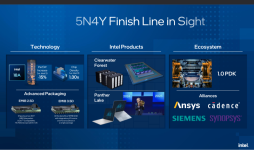
15% improvement in perf/watt, and 1.3X density over Intel 3.

To my eyes that softens the improvement vs. estimated by TechInsights (Semiwiki article), but doesn’t change the picture drastically. PDK 1.0 for Intel 18A seems like a pretty important announcement.

View attachment 2154
Good x Cheap x Fast, that's the magic formula, moreover for foundries.
So, let's say it is good, any guess about cost and cycle time?
 
Intel External foundry revenue was $77m. Down 50% from 2023. This includes wafer sales, packaging, test, and mask services. $77m.

We have a model for how numbers can be this low and why the revenue is down by 50% on a very low number.
 
Last edited:
Pat gets to the heart of the transformation issue when he says:

”Similarly, on the product side, we've done exactly that same analysis. What does a world-class fabulous company look like. And we uncover quite a lot of areas where we don't leverage industry IPs. We're not using our EDA vendors as effectively. We've done too many steppings. We validate versus build-in design quality. So many of these things are steps that we're taking to be a world-class Fabless company, and these are significant structural steps. We also realized that as an IDM 1.0, we were never built for efficiency. We were built for leadership.”
Pat is only talking about the CPU development groups. All of the other chip development groups, except CPU chipsets, have had to be competitive with other fabless companies, because they used TSMC as a fab. Still even chipsets were expected to minimize steppings.
 
There are rumours about low yields for Intel 4: https://www.anandtech.com/show/2149...amp-as-meteor-lake-chips-were-in-short-supply

The article says "we made the decision to accelerate transition of Intel 4 and 3 wafers from our development fab in Oregon to our high volume facility in Ireland, where wafer costs are higher in the near term."

but the question is why they couldn't meet demand in the first place. There are two reasons, firstly low yields of Intel 4, secondly not enough Foveros capacity.
 
In Intel's slide on 5N4Y finish line, it says 18A is 15%/W better than Intel 3.

But per Intel's 2023 10K SEC filing page 14, they claimed 18A is 10%/W better than 20A and 20A is 15%/W better than Intel 3.

Is this an error or did something change? If so, then it might be perceived as defrauding investors in their SEC filing.

https://www.intc.com/filings-report...0000050863-23-000006/0000050863-23-000006.pdf
The disclosure says “up to 15%”, so they’re probably protected by this.
 
The disclosure says “up to 15%”, so they’re probably protected by this.

True… but then how can they honestly call 5 nodes in 4 years? It should be 4 nodes in 4 years!! :)

Its mind boggling that with RibbonFET and Power Via, they’re “only” getting 15%/W improvement vs what TSMC is getting from N3E to A16 which is almost 30%/W

I hope this is not the case, as they’d really be lying to themselves more than even investors.
 
Last edited:
I'm not too clear about the difference/definition between the $15 billion lifetime deal value of committed deals vs the "pipeline" Pat Gelsinger mentioned. Will it be a wishful thinking if the so-called pipeline contains a lot of uncommitted orders or potentials? Do you understand what Pat said?

Pat is not talking foundry speak. Lifetime deal values are pure conjecture unless it is from Intel internal designs.

CC Wei says tape-outs which is easily measurable. Someone on the next investor call should ask Pat how many tape-outs they have in progress for 18A thus far. If CC Wei can see N2 tape-outs Pat should be able to see 18A tape-outs.

I'd be worried if this $15 billion commitment to Intel Foundry is still far from a certainty. But t I think those analysts probably won't ask such questions because there are just too many more urgent and critical questions they haven't gotten a chance to ask yet. One of those urgent questions they didn't have a chance to ask yesterday was the Intel 13th and 14th generation processors' instability problems.
 
Last edited:
Pat is not talking foundry speak. Lifetime deal values are pure conjecture unless it is from Intel internal designs.

CC Wei says tape-outs which is easily measurable. Someone on the next investor call should ask Pat how many tape-outs they have in progress for 18A thus far. If CC Wei can see N2 tape-outs Pat should be able to see 18A tape-outs.
How so? A contract is a contract. If intel says that they have 15B in signed/committed customers, and specifically called out how that is different from their pipeline of clients that have yet to be won. A contract isn't something a customer will just go "nah never mind". If you sign a wafer agreement with TSMC you are locked in. Why would we assume the same doesn't apply to intel's customer especially the one 18A customer who put down a pre-pay assuming intel hits their deliverables as specified in the wafer agreement intel and customer would have signed.

True… but then how can they honestly call 5 nodes in 4 years? It should be 4 nodes in 4 years!! :)
Unless 20A no longer exists why would you come to that conclusion? The performance isn't what makes 18A 18A or 20A 20A. The process changes and enhancements are what makes intel 3 not intel 4, intel 20A not intel 3, and 18A not 20A. By this logic 10nm icelake is 14nm++, and 4LPE is the same as 5LPE because there was no improvement to power performance characteristics. Don't get me wrong if they are weaker than they should be, that is a failure. But just because getting the performance you wanted from the node was not possible within a fixed development timeframe that doesn't mean the process doesn't exist anymore. That is simply not how process definition or development work.
Its mind boggling that with RibbonFET and Power Via, they’re “only” getting 15%/W improvement vs what TSMC is getting from N3E to A16 which is almost 30%/W
If Scotten's estimates of how the processes stack up prove correct, then TSMC is starting from a lower starting point on N3E than intel on intel 3. Also A16 will start high volume production around 1.5-2 yrs after 18A if we take both manufacturers at their word. If A16 couldn't surpass 18A that would be a very bad omen for TSMC's technological competitiveness given A16 is more of a 14A competitor than an 18A competitor.
I hope this is not the case, as they’d really be lying to themselves more than even investors.
Care to elaborate what you mean by this? 5N4Y had the goal of having "process performance per watt parity in 2024 and leadership in 2025" first and foremost. Having 18A be a 26.5% perf/W uplift over intel 3 was a goal, if you fall short of a goal I don't see how that is lying unless intel never had any intention of hitting that target. If you try to hit a target and fail, that is failure not deceitfulness. If you want to call intel out for failing to meet all of their goals I won't argue with you on that count, but I don't see how you arrived at intel "lying to themselves or investors".

Those same bozos erroneously claim N3 yields are terrible and that only with N3E do yields become kind of okay. To say intel 4 yields are poor would be the same as saying TGL and skylake had poor yields. Intel said MTL had a lower DD than either process at launch and MTL also has a smaller die size and lower average utilization by not having things like a GPU on die. If DD was so bad that intel couldn't even have okay yields for MTL over half a year later, large die yield for products like Xeon 6 would be literally 0% because yield rolls of exponentially with die size.
The article says "we made the decision to accelerate transition of Intel 4 and 3 wafers from our development fab in Oregon to our high volume facility in Ireland, where wafer costs are higher in the near term."

but the question is why they couldn't meet demand in the first place. There are two reasons, firstly low yields of Intel 4, secondly not enough Foveros capacity.
Last quarter they literally said they were WLA limited for the purposes of delivering even more unit upside than they did. Also why is it a shocker that a ramping fab has higher wafer cost than one that isn't?! This isn't some exclusive to intel or even the semiconductor industry phenomenon lefty. Ireland is ramping faster than expected and undepreciated intel 4/3 tooling in oregon would start deramping sooner than expected. A double whammy to wafer costs until Ireland is spun up and any intel 4/3 specific tooling in Oregon that isn't getting carried forward presumably gets moved to Ireland.
 
Back
Top