From the Technical Tip Sheet:
“Vertical Channel-All-Around (CAA) IGZO FET less than 50nm CD with High Read Current of 32.8μA/μm (Vth +1V), Well-Performed Thermal Stability up to 120°C for Low Latency, High-Density 2T0C 3D DRAM Application” – Huawei (Paper T2-3)
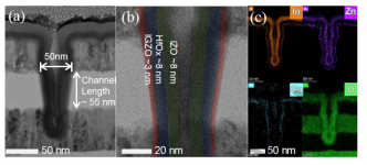
For the first time, Huawei reports on development of high-performance DRAM. They demonstrate a vertical channel-all-around (CAA) IGZO FET, scaled down to an active footprint of less than 50×50nm2 . With optimized IGZO thickness (~3nm) and high-K dielectric (HfOx), high current density of 32.8μA/μm at Vth +1V with subthreshold swing of 92mV/dec is achieved in the IGZO CAA FET with channel length of 55nm and critical dimension (CD) of 50nm. Good thermal stability and reliability is also demonstrated by temperature variation tests and positive-bias-temperature-stress (PBTS) from -40°C to 120°C. Their results show that CAA IGZO FET is a promising candidate for the high-density, high-performance 3D DRAM beyond 1α nodes in the future.
 to repor
“Vertical Channel-All-Around (CAA) IGZO FET less than 50nm CD with High Read Current of 32.8μA/μm (Vth +1V), Well-Performed Thermal Stability up to 120°C for Low Latency, High-Density 2T0C 3D DRAM Application” – Huawei (Paper T2-3)
For the first time, Huawei reports on development of high-performance DRAM. They demonstrate a vertical channel-all-around (CAA) IGZO FET, scaled down to an active footprint of less than 50×50nm2 . With optimized IGZO thickness (~3nm) and high-K dielectric (HfOx), high current density of 32.8μA/μm at Vth +1V with subthreshold swing of 92mV/dec is achieved in the IGZO CAA FET with channel length of 55nm and critical dimension (CD) of 50nm. Good thermal stability and reliability is also demonstrated by temperature variation tests and positive-bias-temperature-stress (PBTS) from -40°C to 120°C. Their results show that CAA IGZO FET is a promising candidate for the high-density, high-performance 3D DRAM beyond 1α nodes in the future.
Attachments
Last edited: