You are currently viewing SemiWiki as a guest which gives you limited access to the site. To view blog comments and experience other SemiWiki features you must be a registered member. Registration is fast, simple, and absolutely free so please, join our community today!
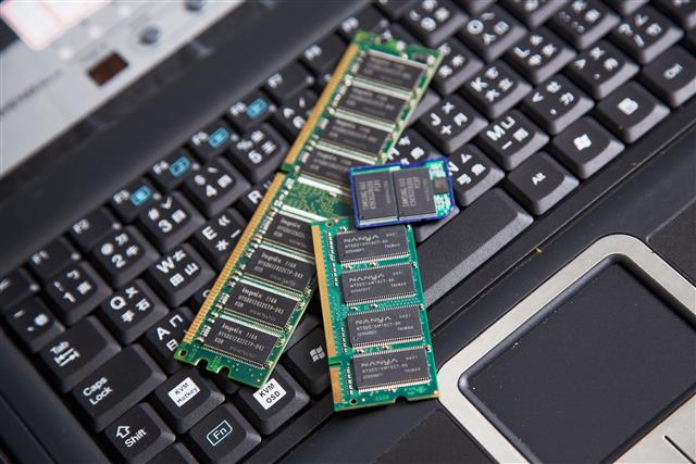
Over the years we keep hearing180nm is obsolete and then when you look at the foundries they still have the 180nm node on their charts. TSMC's webpage still mentions a sizable percentage of wafer starts in 180nm. A quick internet search shows its good for cheaper applications like IoT, Automotive, etc.
#1 So how hot is 180nm today?
#2 Any stats on how many wafer starts in 180nm worldwide?
#3 And the bigger question WHY?
#4 Whats the business viability today?
TSMC investor presentation will tell you what percentage of revenue .18 is. Beyond that I do not know of specific numbers on design starts etc... Other fabs have legacy .18 processes as well. Companies like Semico have reports that includes these types of numbers. Why do you ask?
Hey Dan, hope you are well. Since this COVID thingy its though to just "bump" into people at the Santa Clara Convention Center.
I was just wondering they keep saying 180nm is a mature and cheap node. But we also have the per transistor prices falling with every node advance. So how can 180nm still be viable? And I dont see any design starts at 180nm.
Even early stage startups and academia can ride a shuttle/MPW at say 65nm. That sweet spot should have moved to say 65nm by now.
So are these just respins? Or is there a second tier industry somewhere? Or is it just COVID talk?
Hi Anshuman,
The answer in part is analog. Our design teams have been doing 180nm custom analog sensor signal conditioning and calibration for almost 20 years.
Cheers
Bob
Hi Anshuman,
The answer is all the "unsexy" applications which don't need a ton of compute - automotive, industrial, controls, aerospace, etc.
On most modern 180nm nodes you get logic, analogue and high voltage (200V) design blocks, combined with low mask and wafer costs.
Lets say you needed to make a small form factor 120V motor controller: you can have a high resolution ADCs, high side/low side gate drivers, control logic, a 32-bit microcontroller, single rail voltage input, a CAN transceiver etc. all on one chip with a 50k mask cost and 3k per wafer - very attractive.
To top it all off it will probably be high temperature tolerant so you can attach the package to some part of your equipment chassis and let it run at a junction temperature of 150degC+ and forget about it.
Over the years we keep hearing180nm is obsolete and then when you look at the foundries they still have the 180nm node on their charts. TSMC's webpage still mentions a sizable percentage of wafer starts in 180nm. A quick internet search shows its good for cheaper applications like IoT, Automotive, etc.
#1 So how hot is 180nm today?
#2 Any stats on how many wafer starts in 180nm worldwide?
#3 And the bigger question WHY?
#4 Whats the business viability today?
It's very hot indeed, even prehistoric 200mm foundries are loaded for at least a year+.
Legacy node foundries are seeing record revenues, unseen for decades.
Thank the virus, and an overall resurgence in smart electronics outside of premium segment of iToys, and computers.
Electronics, yet again, paradoxically proves to be a countercyclical industry: in times of crisis, electronics go up, to everyone's bemusement, and confusion.
It was just like that, when 2008 set off a "shanzhai" domestic electronics industry boom in Shenzhen.
180nm node is still widely adopted for a variety of applications. While high performance (HP) ICs will definitely use extremely downscaled nodes, other ICs like RF, analog and/or power applications require the use of larger nodes.
Just quick google search on the market size on the RF industry makes the necessity of such nodes clear.
In addition, it is not about "sexy nodes", it is about practicality.
I will give you an example: Space and high energy physics applications. those are sexy, still present, growing and companies make good money off of them. Guess which nodes they often use?!
They use large process nodes, because they are reliable and well understood. sometimes they even use larger nodes like 1um.
conclusion: large process nodes are still "hot". and they will --very likely- stay so for a long time.
I used to work at a major analog company... half the stuff they were making was still in 180nm
The team I worked on there was making high-reliability parts with a customer-allowed fails per million of 0, so it was invaluable to have a large, very predictable node spec'ed out to within an inch of its life in Cadence. We'd routinely get silicon coming back and testing within 3% of our Virtuoso model's predictions.
The parts didn't have to be fast, they didn't have to be low-power, they didn't have to have a small footprint, and they didn't have to be cheap. But they absolutely needed to work. Accuracy and reliability were the design constraint, not switching speed or power consumption like you see in CPUs or mobile chips.
Getting 180nm capacity was a challenge for us even a couple years ago. We had a little in-house, but everything else 3rd party was contracted out for years like you're seeing. It's been hot for a while.
To top it all off it will probably be high temperature tolerant so you can attach the package to some part of your equipment chassis and let it run at a junction temperature of 150degC+ and forget about it.
Taiwan-based IC distributors have enjoyed strong sales so far in 2020 thanks to clients' keen inventory preparations and Huawei's brisk short-term orders ahead of its trade ban by the US government, and the momentum is expected to continue in 2021, according to sources from the semiconductor...
Globalfoundries and ON Semiconductor have entered into a definitive agreement for ON Semi to acquire a 300mm fab located in East Fishkill, New York, according to the companies.
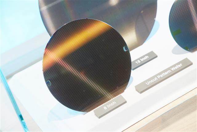
Robust demand for more content for mobile, Internet of Things (IoT), automotive and industrial applications will drive production of 700,000 200mm wafers from 2019 to 2022, a 14% increase, according to SEMI. The increase brings total 200mm wafer fab capacity to 6.5 million wafers per month as...
Toshiba is reportedly seeking to sell its 8-inch fabs in the first quarter of 2021, but the global 8-inch foundry capacity shortages will still hardly be relieved even if the Japanese IDM's fabs are sold to pure-play foundry houses that look to increase their supply to clients, according to...
www.digitimes.com
It all goes towards a single most obvious fact: 180nm on 200mm is the cheapest tapeout on a modern semiconductor process you can get at minimal order quantity of wafers, and under modern, I mean non-prehistoric (where digital tooling flow, digital test, and etc exists.)
And the type of companies looking for a cheapest tapeout possible, are completely ok waiting 6-12 month.
Taiwan-based IC distributors have enjoyed strong sales so far in 2020 thanks to clients' keen inventory preparations and Huawei's brisk short-term orders ahead of its trade ban by the US government, and the momentum is expected to continue in 2021, according to sources from the semiconductor...
Globalfoundries and ON Semiconductor have entered into a definitive agreement for ON Semi to acquire a 300mm fab located in East Fishkill, New York, according to the companies.
Robust demand for more content for mobile, Internet of Things (IoT), automotive and industrial applications will drive production of 700,000 200mm wafers from 2019 to 2022, a 14% increase, according to SEMI. The increase brings total 200mm wafer fab capacity to 6.5 million wafers per month as...
Toshiba is reportedly seeking to sell its 8-inch fabs in the first quarter of 2021, but the global 8-inch foundry capacity shortages will still hardly be relieved even if the Japanese IDM's fabs are sold to pure-play foundry houses that look to increase their supply to clients, according to...
www.digitimes.com
It all goes towards a single most obvious fact: 180nm on 200mm is the cheapest tapeout on a modern semiconductor process you can get at minimal order quantity of wafers, and under modern, I mean non-prehistoric (where digital tooling flow, digital test, and etc exists.)
And the type of companies looking for a cheapest tapeout possible, are completely ok waiting 6-12 month.
")