Array
(
    [content] => 
    [params] => Array
        (
            [0] => /forum/index.php?threads/declining-density-scaling-trend-for-tsmc-nodes.20262/
        )

    [addOns] => Array
        (
            [DL6/MLTP] => 13
            [Hampel/TimeZoneDebug] => 1000070
            [SV/ChangePostDate] => 2010200
            [SemiWiki/Newsletter] => 1000010
            [SemiWiki/WPMenu] => 1000010
            [SemiWiki/XPressExtend] => 1000010
            [ThemeHouse/XLink] => 1000970
            [ThemeHouse/XPress] => 1010570
            [XF] => 2021370
            [XFI] => 1050270
        )

    [wordpress] => /var/www/html
)

Declining density scaling trend for TSMC nodes

Fred Chen

Moderator
A recent Anandtech article https://www.anandtech.com/show/21408/tsmc-roadmap-at-a-glance-n3x-n2p-a16-2025-2026 prompted me to do a trend plot for TSMC density scaling by node (starting from N16), also using https://en.wikipedia.org/wiki/5_nm_process and https://en.wikichip.org/wiki/7_nm_lithography_process as reference.

Here is a brief version:
TSMC node density scaling (brief).png


and here is the full version including more of the N3 and N2 sub-nodes:
TSMC node density scaling (full).png

A classic full node scaling should have a density scaling factor of 2, and we start to fall short of that already at 7nm going to 5nm. It continues dropping going to 3nm, and afterwards, there is practically no scaling (to now). We probably saw signs of this already in the flattening of the SRAM cell size trend. Of course, we expect the others like Samsung and Intel to feel the same difficulty.
 
Last edited:
It would be interesting to do a trend plot comparing nodes every 3 or 4 years rather than yearly; and see how much it changes. How close do they get to 2x performance?
 
Thanks Fred! I really thought N5 to N3 was a bigger jump than that.. It looks like it will take N5 to A16 to match the density improvement that N7 to N5 brought.
 
Thanks Fred! I really thought N5 to N3 was a bigger jump than that.. It looks like it will take N5 to A16 to match the density improvement that N7 to N5 brought.
It would be interesting to do a trend plot comparing nodes every 3 or 4 years rather than yearly; and see how much it changes. How close do they get to 2x performance?
If we do skip nodes, we get something like:
TSMC skip node density scaling.png

N7 vs. N3E would exceed 2x density scaling but still not go as far as N7 vs. N16. A16 vs. N3E, however, would have very little scaling.
Similarly, we can take N5 as the dividing point:
TSMC node density scaling (before and after N5).png

It's a bit more evenly divided (N7 vs. N5, and A16 vs. N5) but both still short of 2x.
We can go further and divide at N7, that gives more than 2x almost evenly divided between before and after N7:
TSMC node density scaling (pre-EUV vs post-EUV).png
 
Last edited:
If we do skip nodes, we get something like:
View attachment 1944
N7 vs. N3E would exceed 2x density scaling but still not go as far as N7 vs. N16. A16 vs. N3E, however, would have very little scaling.
Similarly, we can take N5 as the dividing point:
View attachment 1945
It's a bit more evenly divided (N7 vs. N5, and A16 vs. N5) but both still short of 2x.
We can go further and divide at N7, that gives more than 2x almost evenly divided between before and after N7:
View attachment 1946
Thank you. N10 vs. N7 would be closer to 2x; and A14 vs. N5 might or might not reach 2x, but it's all speculation at this point.
 
No exponential can continue forever but the economic and business urgency requires new products to be meaningfully better every year which that the necessity and invention to find new capability to improve products some how. It’ll drive new direction, maybe transistor density will slow, but between stacking and other innovation we will bring new products to the world for many more years.
 
No exponential can continue forever but the economic and business urgency requires new products to be meaningfully better every year which that the necessity and invention to find new capability to improve products some how. It’ll drive new direction, maybe transistor density will slow, but between stacking and other innovation we will bring new products to the world for many more years.
There's also got to be room to bring down the cost of these latest nodes, and simplify production processes over time. Making nodes like N3 more accessible to more applications.
 
There's also got to be room to bring down the cost of these latest nodes, and simplify production processes over time. Making nodes like N3 more accessible to more applications.
They have had a process exercised on N7 and N4 and likely will apply it on N3.

Once the fab is depreciated the cost structure looks very different as will the price to make healthy margins. If the application has value they can charge it. Since there is competition, he who stays on the older node runs the risk of inferior PPA which often means cost too.
 
None of this should be any surprise because CPP and MP scaling has pretty much stopped -- N2 is pretty much N3 with HNS replacing FinFETs, and A16 is precisely N2 with backside power.

Actually this applies to N5 too, CPP and MP are similar to N3 -- going by our benchmarks the main reason for power/density improvement with N3 is the FlexFin library architecture (e.g. mixing short rows of 1-fin cells with taller rows of 2-fin cells) not the raw process.
 
Actually this applies to N5 too, CPP and MP are similar to N3 -- going by our benchmarks the main reason for power/density improvement with N3 is the FlexFin library architecture (e.g. mixing short rows of 1-fin cells with taller rows of 2-fin cells) not the raw process.
I disagree on that later point. MMP is alot smaller on N3 (as a percentage anyhow). They also use different barriers/liners than N5. The distance between devices is heavily shrunken too necessitating self aligned contacts and a self aligned gate endcap. Even though TSMC is quoting an SRAM density boost of 5% for 1st gen N3, the SEMs show the bitcell area is actually larger than N5, so presumably the density improvement is from improvements to the array control logic. These are all huge changes far beyond just finFLEX. Heck even if you don’t want to look at the SEMs TSMC’s own simulations on an arm core show that the standalone HD lib is most of the way to 2-1. If you were to relax CDs to N5 values that the 1 fin would be at least ~38% larger.

Don’t get me wrong finFLEX is a big deal for maximizing your design, and from a chip designer’s point of view, I bet it is the bee’s knees. My point is more so that finFLEX’s improvements don’t come out of the ether, that the PPA was in a sense always there in the devices, and that finFLEX basically gives you easier access to it. I assume you would know as much, but I just wanted to say that for completeness sake.
I was going by actual synthesized digital layouts (standard cell logic) that we did as opposed to simply looking at the design rules -- and we saw very little improvement in power for N3 compared to N5 using comparable libraries (2-fin), the improvement going to FINflex was considerably bigger and where most of the benefit came from.

The raw process density does improve with N3 but the power changes very little, after all the gates are similar size/length/drive/capacitance per fin but all the metal is crammed closer together giving more capacitance per um, which pretty much cancels out the routing length saving from higher density. Note that digital libraries don't always use the "process minimum" pitch for various reasons including capacitance and ease of access to cells.

N3 did have many improvements compared to N5, including gearing changes to the metal/poly pitches and other tweaks to metal pitches -- some non-obvious where the pitch is bigger in N3.

But the net result is that density improves the most (and a lot of this comes from FINflex), power improves less (and almost all this comes from FINflex).

That's based on real layouts, but of course it will also depend on the circuit, clock speed, supply voltage, library so the results may well be different for other cases.
 
TSMC 28nm is now 22nm. 16nm is now 12nm. N7 is now N6. N5 is now N4, N3 will have little N3x children running around. N2 will be the same. Pretty soon we will just call new process technologies NBT (next big thing).
 
I had the impression the MMP shrink ratio did diminish somewhat: 40->28 for N5 vs 28->23 for N3E.
By alot smaller, I meant that the reduction was significant enough to not be considered "unchanged" seems to be the case with N2/A16 vs N3. The as a percentage was basically me saying that moving to 23 while "only" 5nm is as a percentage a more significant shrink then the raw reduction would indicate. Sorry for the poor wording Fred.

I was going by actual synthesized digital layouts (standard cell logic) that we did as opposed to simply looking at the design rules -- and we saw very little improvement in power for N3 compared to N5 using comparable libraries (2-fin), the improvement going to FINflex was considerably bigger and where most of the benefit came from.

The raw process density does improve with N3 but the power changes very little, after all the gates are similar size/length/drive/capacitance per fin but all the metal is crammed closer together giving more capacitance per um, which pretty much cancels out the routing length saving from higher density. Note that digital libraries don't always use the "process minimum" pitch for various reasons including capacitance and ease of access to cells.

N3 did have many improvements compared to N5, including gearing changes to the metal/poly pitches and other tweaks to metal pitches -- some non-obvious where the pitch is bigger in N3.

But the net result is that density improves the most (and a lot of this comes from FINflex), power improves less (and almost all this comes from FINflex).

That's based on real layouts, but of course it will also depend on the circuit, clock speed, supply voltage, library so the results may well be different for other cases.
All good, I just wanted the TSMC fab people to get recognized for all of their hardwork. Alot of innovation at the process level was needed to do what they did on N3 (even if the end result is less than what folks may be used too). Even on a node that went super smooth like N5 the engineers and techs needed to move mountains to make it happen. For a node that was troubled like N3, they must have had to go to hell and back.
 
By alot smaller, I meant that the reduction was significant enough to not be considered "unchanged" seems to be the case with N2/A16 vs N3. The as a percentage was basically me saying that moving to 23 while "only" 5nm is as a percentage a more significant shrink then the raw reduction would indicate. Sorry for the poor wording Fred.


All good, I just wanted the TSMC fab people to get recognized for all of their hardwork. Alot of innovation at the process level was needed to do what they did on N3 (even if the end result is less than what folks may be used too). Even on a node that went super smooth like N5 the engineers and techs needed to move mountains to make it happen. For a node that was troubled like N3, they must have had to go to hell and back.
I'm not in any way doing down what TSMC have done with N3 (and now N2), their strategy has been excellent -- the problem is they're coming up against fundamental physical limits like gate length and the problems of getting low-resistance access to tinier and tinier transistors crammed together with higher and higher current densities and thinner higher-resistance metal layers and vias. The easiest thing to improve is density, power (from raw process) is more difficult -- most of the gains nowadays are really coming from DTCO improvements and things like COAG and SDB and via pillars. Which of course TSMC also deserve much credit for... ;-)
 
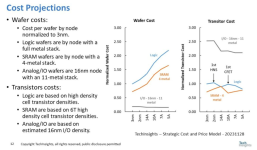
With density scaling slowing so much, and tech being added to create a new node - what is cost per transistor doing between N4/N5, N3, N2, (TSMC not Apple) A16?
 
Back
Top