Array
(
    [content] => 
    [params] => Array
        (
            [0] => /forum/index.php?threads/chinese-2-7-nm-wavelength-ssmb-light-source-disclosed-at-fls2023-in-switzerland.20699/
        )

    [addOns] => Array
        (
            [DL6/MLTP] => 13
            [Hampel/TimeZoneDebug] => 1000070
            [SV/ChangePostDate] => 2010200
            [SemiWiki/Newsletter] => 1000010
            [SemiWiki/WPMenu] => 1000010
            [SemiWiki/XPressExtend] => 1000010
            [ThemeHouse/XLink] => 1000970
            [ThemeHouse/XPress] => 1010570
            [XF] => 2021370
            [XFI] => 1050270
        )

    [wordpress] => /var/www/html
)

Chinese 2.7 nm wavelength SSMB light source disclosed at FLS2023 in Switzerland

Fred Chen

Moderator

Chinese development of the steady-state microbunching (SSMB) light sources for scientific studies and (presumably) lithography has progressed to the point where they now have a design for 2.7 nm, exactly one-fifth of the 13.5 nm EUV wavelength. This would be a shorter wavelength than any ASML can offer.

The SSMB source is far from compact, requiring a 100 meter circumference. However, the power output is in the kW range.

Also, it aggravates the stochastic and electron release issues already demonstrated by 13.5 nm wavelength.

Perhaps the fundamental advantage of this type of light source is that the wavelength is tunable in the design, not determined by the emission spectrum of a specific plasma or gas laser or lamp. They can also do IR, DUV, etc.
 
Last edited:
Chinese development of the steady-state microbunching (SSMB) light sources for scientific studies and (presumably) lithography has progressed to the point where they now have a design for 2.7 nm, exactly one-fifth of the 13.5 nm EUV wavelength. This would be a shorter wavelength than any ASML can offer.

The SSMB source is far from compact, requiring a 100 meter circumference. However, the power output is in the kW range.

Also, it aggravates the stochastic and electron release issues already demonstrated by 13.5 nm wavelength.

Perhaps the fundamental advantage of this type of light source is that the wavelength is tunable in the design, not determined by the emission spectrum of a specific plasma or gas laser or lamp. They can also do IR, DUV, etc.

Very interesting - I think the two large-scale university particle accelerators in the US, SLAC at Stanford and the Wilson Lab at Cornell have been converted into high energy electron and X-RAY sources for this kind of research. At Stanford, it’s the Stanford Synchotron Radiation Lightsource (SSRL) and at Cornell, it’s the Cornell High Energy Synchotron Source (CHESS). Just saw something about Palo Alto-based XLight working with Cornell on next generation lithography. Cornell’s ring is the smallest, 768m in circumference.


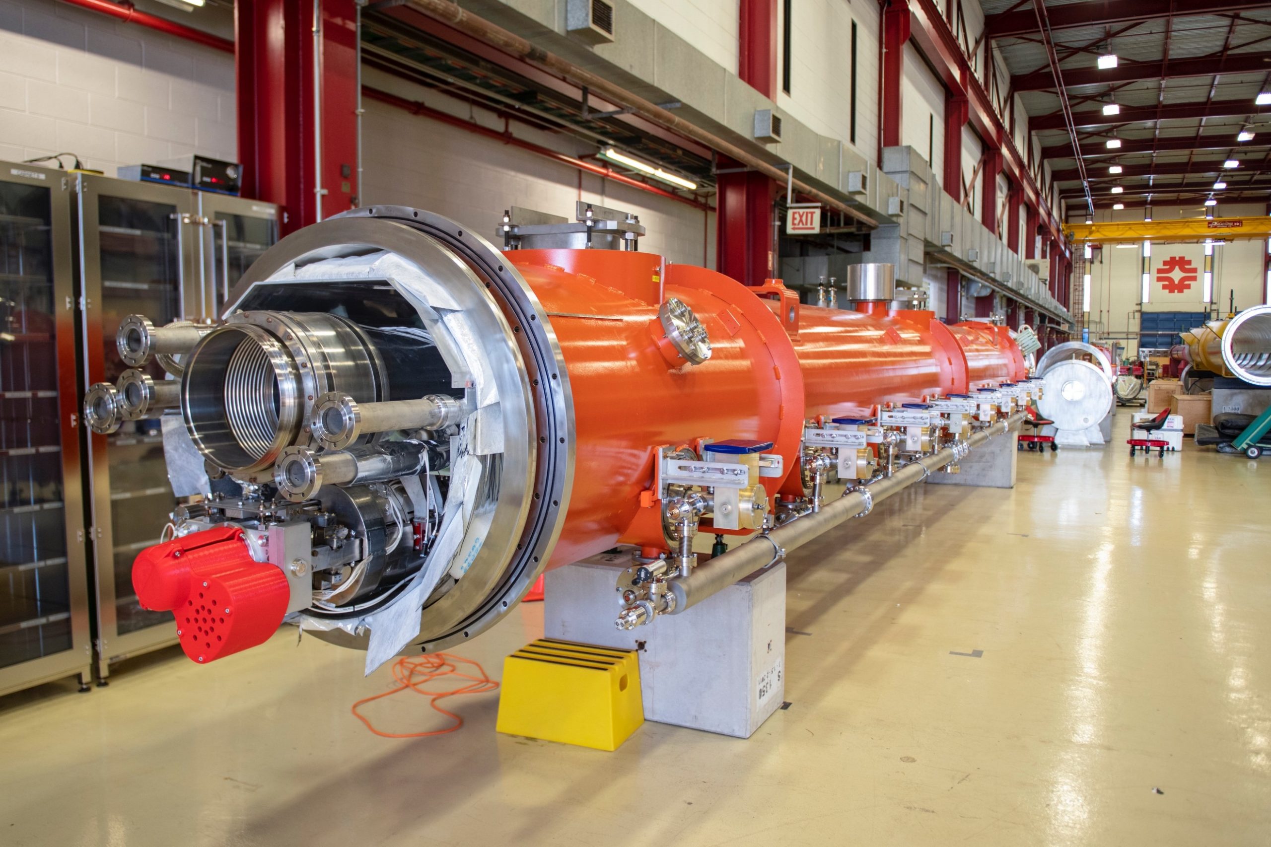
Even the last “working” particle accelerator in the US, FermiLab, is getting in on X-Ray laser imaging and potentially lithography.

 
Last edited:
Very interesting - I think the two large-scale university particle accelerators in the US, SLAC at Stanford and the Wilson Lab at Cornell have been converted into high energy electron and X-RAY sources for this kind of research. At Stanford, it’s the Stanford Synchotron Radiation Lightsource (SSRL) and at Cornell, it’s the Cornell High Energy Synchotron Source (CHESS). Just saw something about Palo Alto-based XLight working with Cornell on next generation lithography. Cornell’s ring is the smallest, 768m in circumference.


Even the last “working” particle accelerator in the US, FermiLab, is getting in on X-Ray laser imaging and potentially lithography.

xLight is looking to build a source similar to the one operated by a Brookhaven-Cornell collaboration (CBETA) https://www.classe.cornell.edu/news...ates-firm-advance-semiconductor-manufacturing

Interestingly, they did not choose the accelerator which was closer.
 
Last edited:

Chinese development of the steady-state microbunching (SSMB) light sources for scientific studies and (presumably) lithography has progressed to the point where they now have a design for 2.7 nm, exactly one-fifth of the 13.5 nm EUV wavelength. This would be a shorter wavelength than any ASML can offer.

The SSMB source is far from compact, requiring a 100 meter circumference. However, the power output is in the kW range.

Also, it aggravates the stochastic and electron release issues already demonstrated by 13.5 nm wavelength.

Perhaps the fundamental advantage of this type of light source is that the wavelength is tunable in the design, not determined by the emission spectrum of a specific plasma or gas laser or lamp. They can also do IR, DUV, etc.

This sounds like it may dovetail nicely with the "Can China get to 3nm" thread.
 
Synchrotron radiation source provides tune-able wavelengths and X-ray Lithography capabilities have been discussed for more than 3 decades and there are several light sources in the world as list below. As we remembered the alternative: MBDW (multiple ebeam direct write) pioneered by Mapper, tsmc Burn Lin-KLA and more were not successful, and David Lam may still work on it now (attached his video in 2023 below). The challenges for advanced lithography for pitch below 40nm are not just in light source only. It is easy to talk and very challenging to achieve production ready scanners.
1722118925739.png

1722118968681.png


I think you need to explain it to people without optics background. Why getting the wavelength smaller no longer pays off.
A short enough wavelength like EUV is ionizing, meaning the absorption releases electrons from atoms in the resist or the ambient gas in the system.

The electrons can travel random distances in the resist while scattering, leading to random local energy dissipation which can be averaged out to a blur. There is no fixed clean number for the blur, although values in the 3-7 nm range are commonly cited. The minimum pitch should be ~7 times the blur for good image quality.

The ambient gas is also ionized, forming an EUV-induced plasma. This plasma can also expose the resist (from electrons, ions, or VUV photons), while also being a source of particles which can obstruct the EUV light or scatter electrons from the plasma.

These are sources of stochastic (random) local exposures of the resist, which can lead to defects, edge placement error, edge roughness, and CD nonuniformity.
 
One of the stochastic processes Fred is referring to is shot-noise.
Since lower wavelength equals higher energy per photon, you need a whole lot less photons at 13.5nm to fully expose the resist than at 193nm.
You cannot control the exact number of photons per time and area and hence not the energy dose a certain area of the resist is exposed to.
Therefore a few (primary) photons more "here" than "there" may lead to a not evenly developed resist. All resist removal and etch processes afterwards will have a hard time.
Yes, I was originally planning to start the explanation with the shot noise. I skipped directly to the ionization since there is a black-and-white threshold for ionization (~10 eV or ~124 nm wavelength). To put it another way, the shot noise can be addressed by dose; a high enough dose would quiet the noise. Earlier in EUV development, this was a big deal, since the source did not have enough power. But now, in the context of developing future synchrotron-based light sources, it may be expected to be no longer an issue.
 
I see.
Would increasing the dose not also risk a higher rate of ionization and lead to more blur?
I assume there is sort of a wavelength-dependent fiure of merit between (intentional) overexposure and blur?
 
I see.
Would increasing the dose not also risk a higher rate of ionization and lead to more blur?
I assume there is sort of a wavelength-dependent fiure of merit between (intentional) overexposure and blur?
Yes, I believe so. But modeling could be a challenge. The standard Gaussian fit to the electron spread may not be appropriate. It could be multi-Gaussian (sum of Gaussians) for example. The latter fit, in fact has been used in electron beam lithography.
 
Last edited:
Back
Top