You are currently viewing SemiWiki as a guest which gives you limited access to the site. To view blog comments and experience other SemiWiki features you must be a registered member. Registration is fast, simple, and absolutely free so please, join our community today!
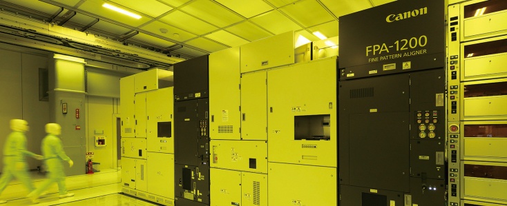
Japanese electronics giant Canon is believed to be in discussions with Indian companies about deals for its proprietary nanoimprint lithography equipment.
evertiq.com
Japanese electronics giant Canon is believed to be in discussions with Indian companies about deals for its proprietary nanoimprint lithography equipment.
Nanoimprint tech stamps chip designs on to silicon wafers rather than etching them using light. As such it offers an alternative to expensive and elusive techniques such as that offered by market leader ASML. Canon says its power consumption is one tenth of the rate of a conventional optical exposure tool.
According to The Economic Times, Canon is negotiating with locally-based firms, believed to include Tata Group, Taiwanese Powerchip Semiconductor Manufacturing Corp (PSMC) and Murugappa group's CG Power. These three companies are especially active in creating a viable Indian foundry sector.
Manabu Yamazaki, Canon Inc’s President and CEO, told ET: “We are in early stages of discussions with Indian and global semiconductor companies who have committed to invest in building semiconductor fabrication units in India as well as others who are expanding electronics manufacturing such as phones and laptops for assembling printed circuit boards and motherboards."
In other news, Canon has also confirmed it will provide skill development training to engineers in India as it provides overseas extended reality (XR) training and web learning.
Good salesmanship. But if nanaimprint will go to an inexperienced operator, and fail publicly, it will be a great bad rep for the technology with well known issues (alignments, stamp endurance, tricky control & metrology.)
I would've thought they will go to the bottom of the market for an easier entry because of the historical opportunity created by the shortage of equipment for old nodes.
It's early stages, it could easily pivot to established node litho tools, e.g., KrF. It depends on how forward looking the companies are. They probably don't want to go through the advanced ArF/EUV hassle.
 evertiq.com