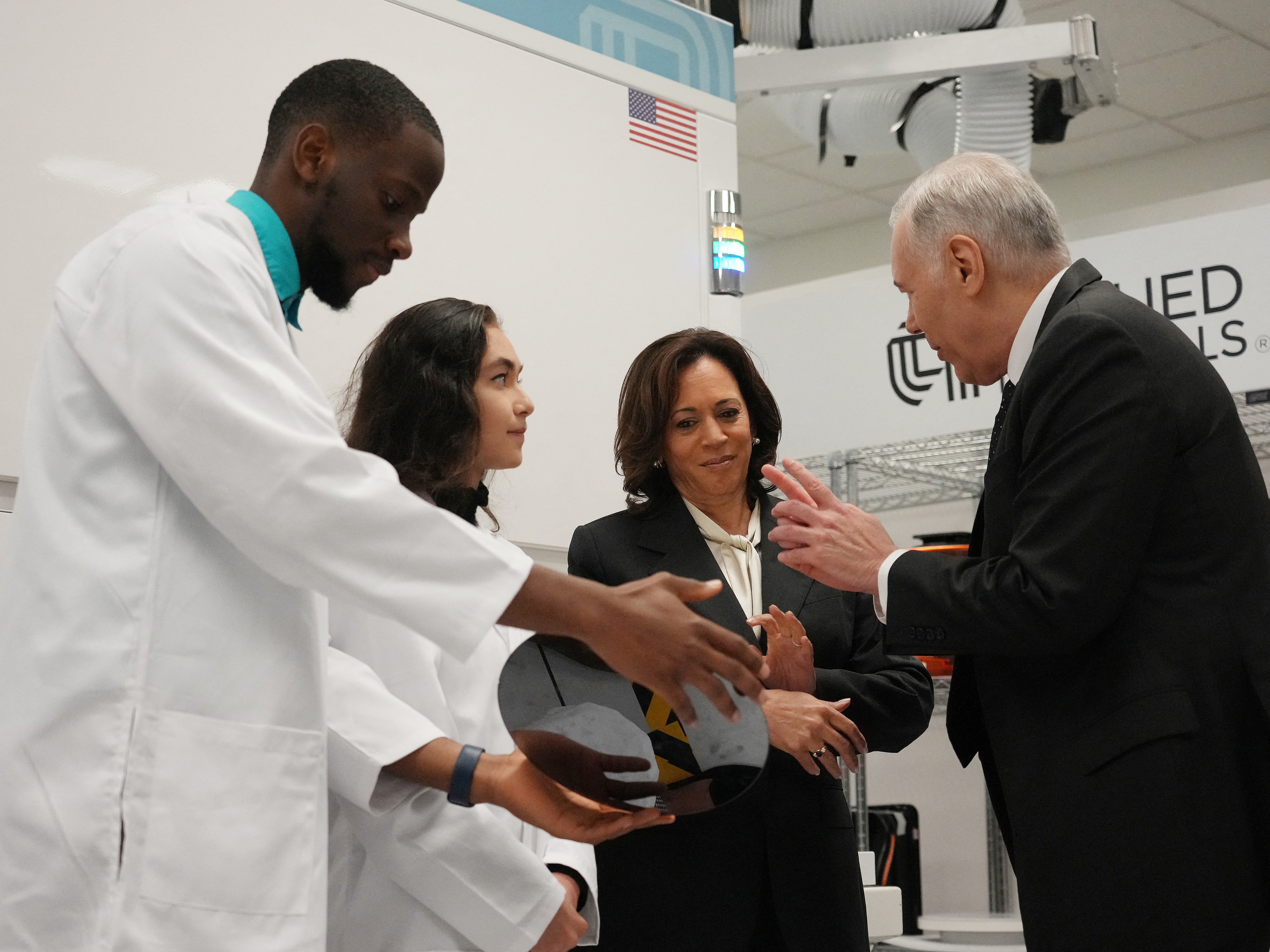
SANTA CLARA, California May 22 (Reuters) - U.S. semiconductor toolmaker Applied Materials Inc (AMAT.O) on Monday said it plans to spend up to $4 billion on a research center in the heart of Silicon Valley to speed up advances in semiconductor manufacturing.
The center based in Sunnyvale, California, will come on line in 2026 and create up to 2,000 engineering jobs, said Applied, the world's biggest maker of tools used in manufacturing chips.
The facility will host about $25 billion of research work over its first decade, pulling together staff from research universities and chipmakers such as Intel Corp (INTC.O), Taiwan Semiconductor Manufacturing Co (2330.TW) and Samsung Electronics Co Ltd (005930.KS), among others.
The announcement comes as the U.S. is trying to bring back advanced semiconductor manufacturing with a $52 billion measure passed last year.
Applied Materials said the new facility, called the Equipment and Process Innovation and Commercialization (EPIC) Center, will be the size of more than three American football fields. Applied said it will invest in it over seven years and wants subsidies from the government through the CHIPS and Science Act.
/cloudfront-us-east-2.images.arcpublishing.com/reuters/ZJM72CYMJ5LLDIRPVMUNBTOY5Q.jpg)
Applied Materials to invest $4 bln in Silicon Valley chip research center
U.S. semiconductor toolmaker Applied Materials Inc on Monday said it plans to spend up to $4 billion on a research center in the heart of Silicon Valley to speed up advances in semiconductor manufacturing.
