Ansys semiconductor simulation tools are certified for UMC's latest wafer-on-wafer (WoW) advanced packaging technology
Key Highlights
- Ansys Redhawk-SC™ and Ansys Redhawk-SC Electrothermal™ have been certified by United Microelectronics Corporation (UMC) to simulate its latest 3D integrated circuit (3D-IC) packaging technology
- Chip designers can leverage Ansys semiconductor solutions to perform multi-die co-analysis for WoW and CoW packaging technology, accelerating and ensuring successful design
PITTSBURGH, PA, October 18, 2023 – Ansys (NASDAQ: ANSS) multiphysics solutions have been certified by global semiconductor foundry UMC to simulate its latest 3D-IC WoW stacked technology, which will improve the power, efficiency and performance of edge AI, graphic processing, and wireless communication systems. The certification empowers more chip designers to employ Ansys’ semiconductor simulation solutions that perform multi-die co-analysis for streamlining and ensuring successful design.
WoW technology consists of silicon wafers, or dies, that are stacked vertically rather than placed horizontally across a board. Built on cloud-optimized infrastructure, Ansys RedHawk-SC™ and Ansys RedHawk-SC Electrothermal™ have the speed, capacity, and predictive accuracy to handle full-chip analysis, including multi-die packages and interconnects for power and signal integrity, thermal profiling, and more. These 3D-IC solutions for multiphysics analysis fit into a larger set of comprehensive Ansys solutions for board and system electrothermal analysis, including Ansys SIwave™ and Ansys Icepak™.

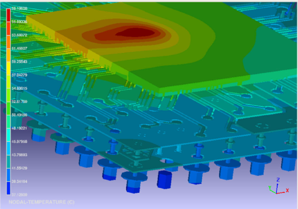
ANSYS® RedHawk-SC Electrothermal™ simulation result showing the temperature distribution of a chip and package assembly.
“We’re pleased with the result of our collaboration with Ansys in the delivery of UMC technology reference flow, which empowers customers to address growing performance, reliability, and power demands for cloud and data center applications,” said Osbert Cheng, vice president of device technology development and design support at UMC. “The collaborative efforts combining Ansys’ comprehensive chip-package co-analysis solutions with UMC’s advanced chip-stacking technology address complex multiphysics challenges in 3D-IC packaging technologies.”
“Ansys and UMC’s 3D-IC solutions address complex multiphysics challenges to meet stringent power, performance, thermal and reliability requirements,” said John Lee, vice president and general manager of the electronics, semiconductor, and optics business unit at Ansys. “Ansys’ dual-approach with both chip- and system-aware design solutions enable mutual customers to accelerate design convergence with greater confidence from small, delicate details at chip level to system-level design challenges.”
About Ansys
Our Mission: Powering Innovation that Drives Human AdvancementTMWhen visionary companies need to know how their world-changing ideas will perform, they close the gap between design and reality with Ansys simulation. For more than 50 years, Ansys software has enabled innovators across industries to push boundaries by using the predictive power of simulation. From sustainable transportation to advanced semiconductors, from satellite systems to life-saving medical devices, the next great leaps in human advancement will be powered by Ansys.
Ansys and any and all ANSYS, Inc. brand, product, service and feature names, logos and slogans are registered trademarks or trademarks of ANSYS, Inc. or its subsidiaries in the United States or other countries. All other brand, product, service and feature names or trademarks are the property of their respective owners.
Link to Press Release
