Array
(
    [content] =>
    [params] => Array
        (
            [0] => /forum/threads/nvidia-allegedly-eyeing-samsung%E2%80%99s-3nm-process-node-for-geforce-rtx-50-series-gpus.17147/
        )

    [addOns] => Array
        (
            [DL6/MLTP] => 13
            [Hampel/TimeZoneDebug] => 1000070
            [SV/ChangePostDate] => 2010200
            [SemiWiki/Newsletter] => 1000010
            [SemiWiki/WPMenu] => 1000010
            [SemiWiki/XPressExtend] => 1000010
            [ThemeHouse/XLink] => 1000970
            [ThemeHouse/XPress] => 1010570
            [XF] => 2021770
            [XFI] => 1050270
        )

    [wordpress] => /var/www/html
)
Guests have limited access.
Join our community today!
Join our community today!
You are currently viewing SemiWiki as a guest which gives you limited access to the site. To view blog comments and experience other SemiWiki features you must be a registered member. Registration is fast, simple, and absolutely free so please, join our community today!
You are using an out of date browser. It may not display this or other websites correctly.
You should upgrade or use an alternative browser.
You should upgrade or use an alternative browser.
NVIDIA Allegedly Eyeing Samsung’s 3nm Process Node for GeForce RTX 50 Series GPUs
- Thread starter VCT
- Start date
Mooredaddy
Well-known member
I find this hard to believe although I don’t have the sources others do. Samsungs foundry division seems to be plagued by horrible management, horrific yields and questionable PDK’s. In addition Nvidia can’t afford to play the cost game as they did on Samsung 8nm as AMD is hot on their heals and due to pass them in rasterization performance next gen IMO. Chiplets are allowing AMD to off load cache from the main compute die and nvidia is rapidly running out of real estate for cache on their monolithic dies. If Nvidia tries to cheap out on what I believe will be an inferior node at Samsung vs N3E they are going to have even bigger issues. All my opinion of course.
NVIDIA is designing to TSMC N3E. Samsung 3nm GAA is still in the development phase. The problem with being on the bleeding edge of semiconductor technology is that there is a lot of bleeding, absolutely.
Here is a design challenge when moving to a GAA process. FinFETs are open source so there is a huge amount of community support for PDKs and other design necessities. BSIM models for example: https://en.wikipedia.org/wiki/BSIM
For GAA, each foundry will have to create their own models and each EDA/IP company will need to be able to work with all of these different models. This will be a huge advantage for TSMC since the majority of customers go to TSMC first. TSMC also has the advantage of having a diverse customer base so you know their PDKs will be well tested for different markets. TSMC also has Apple (SoC, Arm) and AMD (CPU/GPU/FPGA) as close PDK development partners.
hist78
Well-known member
NVIDIA is designing to TSMC N3E. Samsung 3nm GAA is still in the development phase. The problem with being on the bleeding edge of semiconductor technology is that there is a lot of bleeding, absolutely.
Here is a design challenge when moving to a GAA process. FinFETs are open source so there is a huge amount of community support for PDKs and other design necessities. BSIM models for example: https://en.wikipedia.org/wiki/BSIM
For GAA, each foundry will have to create their own models and each EDA/IP company will need to be able to work with all of these different models. This will be a huge advantage for TSMC since the majority of customers go to TSMC first. TSMC also has the advantage of having a diverse customer base so you know their PDKs will be well tested for different markets. TSMC also has Apple (SoC, Arm) and AMD (CPU/GPU/FPGA) as close PDK development partners.
By the estimates done by Digitimes and Bloomberg, Nvidia is the #6 largest TSMC client in 2021 with only a small 2.83% share. In reality Nvidia doesn't have too much volume that can be moved from TSMC to Samsung measured by the 2021 number. Nvidia may have more orders placed at TSMC in 2022 but I think the Nvidia's business share over the overall TSMC revenue probably hasn't changed too drastically for 2022.
Nvidia always practices multi sourcing or dual sourcing strategies to get the best deal and the best capacity allocation. But for such small percentage at TSMC, if Nvidia doesn't place more orders at TSMC in the coming years, Nvidia may drop further in the ranking. Nvidia may become too small to ask to be treated as good as Mediatek, AMD, Qualcomm, Broadcom, or even Intel.
AMD Becomes TSMC's Third Largest Customer
But Apple maintains undisputable lead.
Last edited:
By the estimates done by Digitimes and Bloomberg, Nvidia is the #6 largest TSMC client in 2021 with only a small 2.83% share. In reality Nvidia doesn't have too much volume that can be moved from TSMC to Samsung measured by the 2021 number. Nvidia may have more orders placed at TSMC in 2022 but I think the Nvidia's business share over the overall TSMC revenue probably hasn't changed too drastically for 2022.
Nvidia always practices multi sourcing or dual sourcing strategies to get the best deal and the best capacity allocation. But for such small percentage at TSMC, if Nvidia doesn't place more orders at TSMC in the coming years, Nvidia may drop further in the ranking. Nvidia may become too small to ask to be treated as good as Mediatek, AMD, Qualcomm, Broadcom, or even Intel.
AMD Becomes TSMC's Third Largest Customer
But Apple maintains undisputable lead.www.tomshardware.com
Nvidia moved back to TSMC at 5nm, 4nm and 3nm so their TSMC customer share will increase in the coming years. Nvidia is doing very large and complex chips, and given they bounce around foundries they do not have inner circle privileges at TSMC. Bottom line: It will take Nvidia longer to get to TSMC HVM.
I heard that Nvidia did a pre payment for N5 and N3 but I have not been able to verify it.
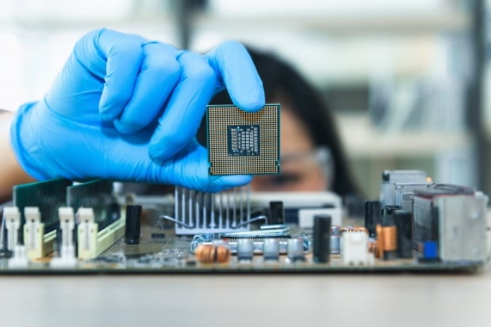
Samsung Electronics Co., the world’s largest memory chipmaker, will make semiconductors with the industry’s most advanced 3-nanometer process node for its clients, including Nvidia, Qualcomm Technologies, IBM and China’s Baidu.
The South Korean tech giant is jointly developing advanced chips with five to six fabless clients for supply in large quantities from as early as 2024, people familiar with the matter said on Tuesday.
Samsung will use its 3 nm technology to manufacture graphics processing units (GPUs) for Nvidia, central processing units (CPUs) for IBM, smartphone application processors for Qualcomm and artificial intelligence chips used in cloud data centers for Baidu, sources said.
These customers are known to have selected Samsung as a consignment producer in consideration of the Korean chipmaker’s 3 nm process technology as well as their need to secure multiple suppliers, the sources said.
Market watchers said Samsung hopes to leverage its 3 nm technology to overtake its bigger foundry rival Taiwan Semiconductor Manufacturing Co. (TSMC) in the contract chipmaking business.

Samsung executives celebrate the production of the world's first 3 nm GAA chips
Samsung is the world’s top player in the memory sector. In the contract manufacturing business, however, it is a distant second with a low double-digit market share after TSMC, which controls more than half of the global foundry market.
HEATED RACE FOR 3 NM PROCESS NODE
The world’s two largest foundry chipmakers, TSMC and Samsung, have been in a heated race for the 3 nm process node, currently, the industry’s narrowest circuitry, to manufacture chips with increased transistor density, faster data speed and reduced power consumption.
In June, Samsung said it has kicked off mass production of advanced chips based on the industry’s smallest process node as a global first to narrow its gap with TSMC.
In the chipmaking process, nanometer refers to the circuitry size of the transistors that can be packed on a chip. The lower the nanometer number, the more advanced the technology, promising a faster computing speed, higher performance and lower power use.
According to Samsung, its 3 nm technology improves power efficiency and chip performance by 45% and 23%, respectively, compared with its earlier 5 nm technology.

TSMC is the world's largest foundry player
Further, Samsung said it plans to commercialize more advanced 2 nm GAA technology by 2025 to become the top player in the foundry market by 2030.
With the demand for high-performance computing (HPC) chips used in supercomputers and computer clusters rising, foundry competition is heating up. US tech giant Intel Corp. has also thrown down the gauntlet to jump into the foundry business, a growing sector that manufactures cutting-edge chips for fabless firms, including chip designers.
TSMC, which counts Apple and Advanced Micro Devices (AMD) among its major customers, said earlier this week its new factory in the US state of Arizona will have a 3 nm facility as well as 5 nm lines.
Analysts said growing geopolitical risks such as the deepening conflict between the US and China are leading fabless companies to seek multiple suppliers.
“Some companies are cutting down on their transactions with Taiwanese companies. Instead, they are looking for a second and a third supplier in other countries such as Samsung,” said an official at a back-end process firm.
Samsung has contract chipmaking facilities in five locations around the world: Giheung, Hwaseong and Pyeongtaek in Korea; and Austin and Taylor in the US state of Texas.
In August, the US government announced that it would ban the export of certain semiconductors and equipment containing US technology to China amid the growing conflict between the two countries.
Samsung runs a NAND chip manufacturing facility in the Chinese city of Xian, but it has been given a one-year reprieve from the US government on the import of chip equipment to the plant.
The South Korean tech giant is jointly developing advanced chips with five to six fabless clients for supply in large quantities from as early as 2024, people familiar with the matter said on Tuesday.
Samsung will use its 3 nm technology to manufacture graphics processing units (GPUs) for Nvidia, central processing units (CPUs) for IBM, smartphone application processors for Qualcomm and artificial intelligence chips used in cloud data centers for Baidu, sources said.
These customers are known to have selected Samsung as a consignment producer in consideration of the Korean chipmaker’s 3 nm process technology as well as their need to secure multiple suppliers, the sources said.
Market watchers said Samsung hopes to leverage its 3 nm technology to overtake its bigger foundry rival Taiwan Semiconductor Manufacturing Co. (TSMC) in the contract chipmaking business.
Samsung executives celebrate the production of the world's first 3 nm GAA chips
Samsung is the world’s top player in the memory sector. In the contract manufacturing business, however, it is a distant second with a low double-digit market share after TSMC, which controls more than half of the global foundry market.
HEATED RACE FOR 3 NM PROCESS NODE
The world’s two largest foundry chipmakers, TSMC and Samsung, have been in a heated race for the 3 nm process node, currently, the industry’s narrowest circuitry, to manufacture chips with increased transistor density, faster data speed and reduced power consumption.
In June, Samsung said it has kicked off mass production of advanced chips based on the industry’s smallest process node as a global first to narrow its gap with TSMC.
In the chipmaking process, nanometer refers to the circuitry size of the transistors that can be packed on a chip. The lower the nanometer number, the more advanced the technology, promising a faster computing speed, higher performance and lower power use.
According to Samsung, its 3 nm technology improves power efficiency and chip performance by 45% and 23%, respectively, compared with its earlier 5 nm technology.
TSMC is the world's largest foundry player
Further, Samsung said it plans to commercialize more advanced 2 nm GAA technology by 2025 to become the top player in the foundry market by 2030.
With the demand for high-performance computing (HPC) chips used in supercomputers and computer clusters rising, foundry competition is heating up. US tech giant Intel Corp. has also thrown down the gauntlet to jump into the foundry business, a growing sector that manufactures cutting-edge chips for fabless firms, including chip designers.
TSMC, which counts Apple and Advanced Micro Devices (AMD) among its major customers, said earlier this week its new factory in the US state of Arizona will have a 3 nm facility as well as 5 nm lines.
Analysts said growing geopolitical risks such as the deepening conflict between the US and China are leading fabless companies to seek multiple suppliers.
“Some companies are cutting down on their transactions with Taiwanese companies. Instead, they are looking for a second and a third supplier in other countries such as Samsung,” said an official at a back-end process firm.
Samsung has contract chipmaking facilities in five locations around the world: Giheung, Hwaseong and Pyeongtaek in Korea; and Austin and Taylor in the US state of Texas.
In August, the US government announced that it would ban the export of certain semiconductors and equipment containing US technology to China amid the growing conflict between the two countries.
Samsung runs a NAND chip manufacturing facility in the Chinese city of Xian, but it has been given a one-year reprieve from the US government on the import of chip equipment to the plant.
Samsung to make 3 nm chips for Nvidia, Qualcomm, IBM, Baidu - KED Global
Samsung Electronics Co., the world’s largest memory chipmaker, will make semiconductors with the industry’s most advanced 3-nanometer process node
www.kedglobal.com