Array
(
    [content] => 
    [params] => Array
        (
            [0] => /forum/index.php?threads/are-samsung%E2%80%99s-3nm-gaa-volume-production-yields-closer-to-25-or-70.16269/
        )

    [addOns] => Array
        (
            [DL6/MLTP] => 13
            [Hampel/TimeZoneDebug] => 1000070
            [SV/ChangePostDate] => 2010200
            [SemiWiki/Newsletter] => 1000010
            [SemiWiki/WPMenu] => 1000010
            [SemiWiki/XPressExtend] => 1000010
            [ThemeHouse/XLink] => 1000970
            [ThemeHouse/XPress] => 1010570
            [XF] => 2021370
            [XFI] => 1050270
        )

    [wordpress] => /var/www/html
)

Are Samsung’s 3nm GAA Volume Production Yields Closer to 25% or 70%

Samsung has said they are building (3) 3nm fabs so they have high hopes. Based on the numbers I have seen Samsung 3nm is not competitive to TSMC N3 or Intel 3 and the design learning curve for GAA is still an issue so I do not expect the big semiconductor companies to bet their HVM products on Samsung 3nm.

In my opinion TSMC N2, Samsung 3nm, and Intel 20A will be yield learning nodes with few customers. Intel proper will be the only 20A customer and it will be CPU tiles only. TSMC N2 will be a like like 20nm and 10nm where only Apple did HVM and if you look at the latest TSMC financials there is no revenue attached to those nodes.
 
What are the odds that after years of pathetically low yields from Samsung's 5nm and 4nm chips, which are using DECADES OLD FinFET technology, that suddenly their soon to be released BRAND NEW Gate-All-Around (GAA) technology will have yields greater than 35%.

http://koreabizwire.com/samsung-expected-to-announce-mass-production-of-3nm-chip-next-week/221816

The bragging right is important to certain companies and Samsung is one of them. Does that change any competitive landscape? Probably not. Foundry customers spend big money and take so much risk to develop and make a product. They are sophisticated enough to tell what's real and what's important to them.
 
Samsung has said they are building (3) 3nm fabs so they have high hopes. Based on the numbers I have seen Samsung 3nm is not competitive to TSMC N3 or Intel 3 and the design learning curve for GAA is still an issue so I do not expect the big semiconductor companies to bet their HVM products on Samsung 3nm.

In my opinion TSMC N2, Samsung 3nm, and Intel 20A will be yield learning nodes with few customers. Intel proper will be the only 20A customer and it will be CPU tiles only. TSMC N2 will be a like like 20nm and 10nm where only Apple did HVM and if you look at the latest TSMC financials there is no revenue attached to those nodes.

Eight weeks ago, sources were claiming Samsung’s 3nm GAA yields were 15%, including sources published here at SemiWiki.

It’s hard to imagine those yields have improved much since then, considering the additional complexity of their GAA construction.

https://wccftech.com/samsung-3nm-gaa-worse-yields-than-4nm/?beta=1
 
I'm wondering how much impacts or involvement on Samsung's 3nm from IBM?

It will be interesting if the reported Japan-US 2nm research and manufacturing project will use IBM's process technology.

IBM keeps conducting semiconductor manufacturing process research since it became a fabless company several years ago. As far as I know IBM is the only fabless company doing that.
 
Last edited:
They claimed 3nm GAA will be in production in 1H/22, so they'll make an announcement at the end of June just to say that they hit the milestone, regardless of what the yield is (which is probably low).

Samsung did the same at 10nm. The had to be first at all costs. When the announcement went live I talked to some friends at QCOM and they said 10nm yield was in single digits and they were getting good die versus wafers from Samsung to hide it.

It is a cultural thing, being first no matter what the costs. As I have said before, Samsung's biggest foundry market segment is the NOT TSMC business. Intel is now competing for that market so Samsung is in serious foundry trouble, my opinion.

I don't see either Samsung or Intel as a serious threat to TSMC with the FinFET business. GAA may be another story but if I had to bet on a winner it would be TSMC. The TSMC ecosystem and huge customer support is a force of nature, absolutely.

After years of poor Exynos performance and user complaints, and according to news/rumors, Samsung may put their Exynos SoC on hold, or even cancel, and use outside SoC's from Qualcomm, MediaTek, or similar.

If the demise of Exynos is true, and if sufficient foundry customers can't be convinced to come back, what internal Samsung device might use their 3nm process?
They could still court other makers of SoC's to use their fabs and then pull some kind of the very old IBM trick of being allowed to fab the exact same thing for themselves for a small licensing fee.

Question - when ARM creates a new ARM core or ARM IP and then goes to TSMC to fab test versions of it on the latest nodes.. do they also do this at Samsung or not?
 
Question - when ARM creates a new ARM core or ARM IP and then goes to TSMC to fab test versions of it on the latest nodes.. do they also do this at Samsung or not?

I don’t see why not, unless ARM’s test metrics are sensitive to excessive heat.
 
They could still court other makers of SoC's to use their fabs and then pull some kind of the very old IBM trick of being allowed to fab the exact same thing for themselves for a small licensing fee.

Question - when ARM creates a new ARM core or ARM IP and then goes to TSMC to fab test versions of it on the latest nodes.. do they also do this at Samsung or not?

Yes, Samsung is an Arm customer and partner. Synopsys SRAM as well and some SerDes stuff All belong on leading edge process test chips for yield and performance check.
 
Question - when ARM creates a new ARM core or ARM IP and then goes to TSMC to fab test versions of it on the latest nodes.. do they also do this at Samsung or not?
Some clarifying points:
1) ARM develops physical IP design in addition to Soft IP (Physical is their std cell libraries and memory IP, which they license out as POP kits for their CPU / GPU soft IP; sometimes also GPIOs, but that is about it). ARM have made POP kits available on Samsung S7LPP and S5LPE from what I've seen announced at previous SFFs, but unclear about anything more recent.
2) ARM very occasionally will develop a POC or development vehicle, that includes physical implementations of their CPU or GPU IP; typically this is done only when there is a new ISA change and they want to seed development community with this device for early software development outside of their own internal migration.

Otherwise, ARM only develops their IP on FPGAs / emulation environments and licenses that soft IP to customers, who are the first to physically implement it, either with Foundry physical IP, or with POP kits. I can think of one instance in the past decade where ARM put an early CPU on N10 in support of a specific customer, but otherwise when you see claims from TSMC or Samsung Foundry about ARM CPU performance, it is the Foundry doing the implementation of that IP (Cortex A72, A53, etc), not ARM. They might use a Foundry PDK to validate that their IP meets specific PPA claims, but that doesn't mean they are going to drop that onto a shuttle.

You would see ARM cores used for PPA claims at events like SNUG / CDNLive / DAC, but again these are typically a customer (Mediatek), the EDA companies, or the Foundries themselves doing the presentation, and maybe ARM is there as a partner on the project. ARM has also done some interesting testchips to test concepts like 3D stacking / core folding (Trishul) but they are using proven CPU or fabric IP for that (keeps the bugs limited to their POC vs the IP), and again it is unclear to me if they took those projects from a converged design (what they share in publications) to actual silicon.
 
This is the translated Korean version of the article https://www.thelec.kr/news/articleView.html?idxno=17300 which has some info. that is left out in the English version.

Note: "It is observed that the timing of mass production using the actual 3nm process may need to be watched a little longer. Some say that the time for full-scale mass production of GAA 3nm by Samsung Electronics will be the end of this year at the earliest or the first half of next year at the latest."

Samsung Electronics begins 'trial production' of 3-nano foundry... The first customer is a Chinese ASIC company
  • By Jang Kyung-yoon
  • Approval 2022.06.28 09:10
Industry's first 3-nano process applied with GAA process... Started trial production The first customer secured some reserve quantities from Qualcomm, a US semiconductor company for bitcoin mining in China .

Samsung Electronics will start 'trial production' of the 3-nm (nm) foundry process as early as this week. The first customer is said to be a Chinese bitcoin mining semiconductor company. It is reported that Qualcomm of the United States has also received a 'reserve' (reservation) that it can produce some quantities on consignment. It is not 'mass production' in the general sense, but the industry's evaluation is that it is meaningful in that it is the world's first 3-nm trial production using the GAA (gate-all-around) process.

According to the semiconductor industry on the 28th, Samsung Electronics plans to start trial production of 3nm products using the GAA process as early as this week.

GAA is a next-generation transistor structure that utilizes four sides, unlike the existing finFET structure that uses three sides of a channel through which current flows. Compared to the FinFET structure, it has more precise current control capability and high power efficiency, so it is considered an essential technology to realize ultra-fine semiconductor line width.

The first customer of the 3nm GAA process is known as PanSemi, a fabless chip for Bitcoin mining (ASIC) in China. It is known that the company has reached an agreement with Qualcomm, the largest customer of Samsung Foundry, that it can entrust the production of chips using the 3-nm process at any time.

This is interpreted as a strategy to secure Samsung Electronics' 3nm process margin in advance in case a problem arises in the 3nm process of TSMC, a Taiwanese foundry company. Previously, Qualcomm tried to produce a mobile AP (application processor) using Samsung Electronics' 3nm process, but Samsung Electronics failed to meet the yield conditions and thus entrusted the supply to TSMC.

Samsung Electronics has set the goal of mass-producing the world's first 3-nano GAA process in the first half of this year. This position was reconfirmed in a conference call after the announcement of the first quarter results. With this trial production, Samsung Electronics' promise of '3nm mass production in the first half' is expected to be kept. However, it is known that this production is close to trial production, which is made by testing the product, rather than mass production in the general sense.

The industry believes that the fact that Samsung Electronics is actually producing the world's first GAA 3nm process is significant. Samsung Electronics has been pointed out that the 3nm process development is not smooth due to the lack of IP (intellectual property) related to the 3nm process and sluggish yield. Recently, there has also been an observation that the 3nm process mass production schedule has been postponed. Samsung Electronics countered this, saying, "The 3-nano mass production schedule is proceeding as scheduled without any setbacks, and mass production will begin in the first half of the year."

An industry official said, "Even at the trial production stage, it can be very helpful for Samsung Electronics to secure customers by increasing the technology and yield of the 3nm GAA process." It still appears to be unclear." It is observed that the timing of mass production using the actual 3nm process may need to be watched a little longer. Some say that the time for full-scale mass production of GAA 3nm by Samsung Electronics will be the end of this year at the earliest or the first half of next year at the latest.

Meanwhile, TSMC is preparing for mass production of 3nm process (N3) based on FinFlex. Finflex is a technology that provides the existing FinFET structure customized according to various options desired by chip designers. For example, based on the 3N process, 3-2 FIN with the highest frequency, 2-2 FIN with a balance between performance and efficiency, and 1-2 FIN with emphasis on power efficiency can be mixed and used in the same die. The basic N3 process will be mass-produced from the second half of this year, and the improved process will be mass-produced after that.
At the beginning of this year, TSMC also raised a problem that the 3nm process yield was lower than expected, but like Samsung Electronics, it emphasized that there is no setback in the plan. TSMC Chairman Mark Liu said at a shareholder briefing held on the 6th of this month, "We will start mass production of the 3N process in the second half of this year, and the improved process will begin mass production one year after that."
 
This is the translated Korean version of the article https://www.thelec.kr/news/articleView.html?idxno=17300 which has some info. that is left out in the English version.

Note: "It is observed that the timing of mass production using the actual 3nm process may need to be watched a little longer. Some say that the time for full-scale mass production of GAA 3nm by Samsung Electronics will be the end of this year at the earliest or the first half of next year at the latest."

Samsung Electronics begins 'trial production' of 3-nano foundry... The first customer is a Chinese ASIC company

So it's more like Intel Loihi 2 production. Intel used their early 4nm fab to produce small neuromorphic chips. Maybe same purpose(learning curve).
 
It's official:


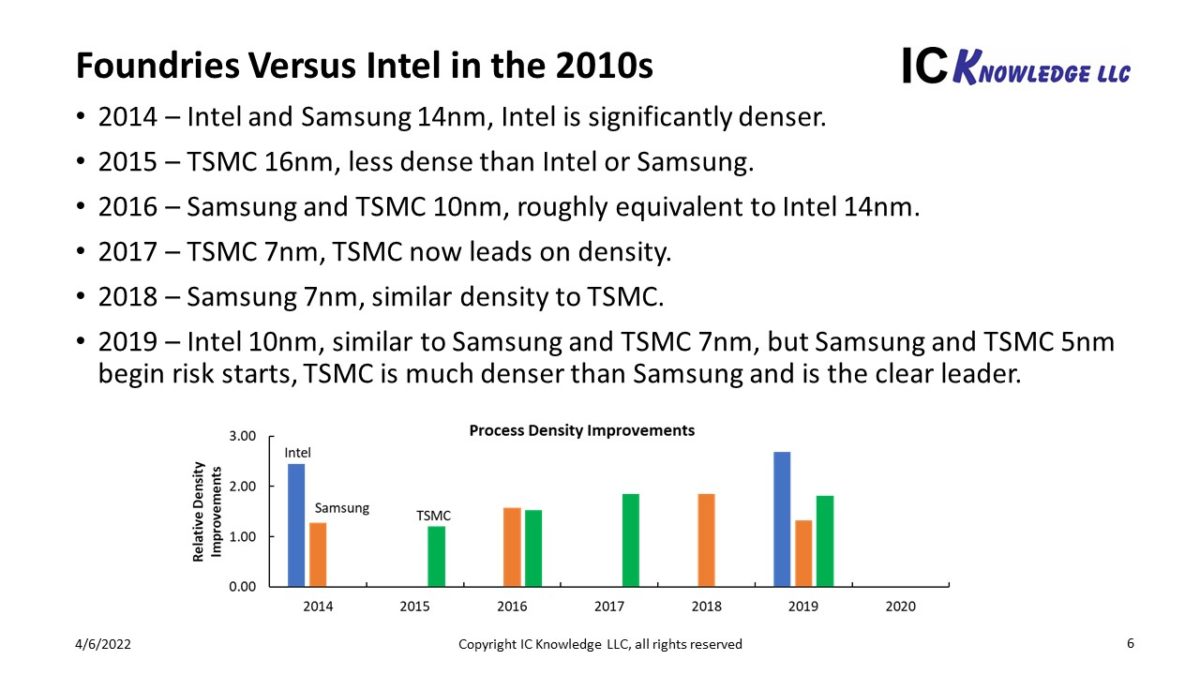
I still have not heard of anyone working with this process. And here is the comparison Scott made:

 
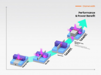
Samsung press release has a cool infographic, evolution of FET (and difference between nanowire and nanosheet, pretty helpful)
 

Attachments

  • Screenshot 2022-06-30 at 09-18-15 Samsung Begins Chip Production Using 3nm Process Technology ...png
    Screenshot 2022-06-30 at 09-18-15 Samsung Begins Chip Production Using 3nm Process Technology ...png
    356.8 KB · Views: 179
It's official:


I still have not heard of anyone working with this process. And here is the comparison Scott made:

hey Dan,

There are some nice SEM images on the breakdown of A15 bionic. Is there a chance we get Scotten to revisit this?

 
Back
Top