Array
(
    [content] => 
    [params] => Array
        (
            [0] => /forum/index.php?threads/tsmc-announces-updates-for-tsmc-arizona.17156/
        )

    [addOns] => Array
        (
            [DL6/MLTP] => 13
            [Hampel/TimeZoneDebug] => 1000070
            [SV/ChangePostDate] => 2010200
            [SemiWiki/Newsletter] => 1000010
            [SemiWiki/WPMenu] => 1000010
            [SemiWiki/XPressExtend] => 1000010
            [ThemeHouse/XLink] => 1000970
            [ThemeHouse/XPress] => 1010570
            [XF] => 2021370
            [XFI] => 1050270
        )

    [wordpress] => /var/www/html
)

TSMC Announces Updates for TSMC Arizona

Daniel Nenni

Admin
Staff member
TSMC Fab AZ.jpg

PHOENIX, Arizona, Dec. 6, 2022 – TSMC (TWSE: 2330, NYSE: TSM) today announced that
in addition to TSMC Arizona’s first fab, which is scheduled to begin production of N4 process
technology in 2024, TSMC has also started the construction of a second fab which is scheduled to
begin production of 3nm process technology in 2026. The overall investment for these two fabs
will be approximately US$40 billion, representing the largest foreign direct investment in Arizona
history and one of the largest foreign direct investments in the history of the United States.

In addition to the over 10,000 construction workers who helped with construction of the site,
TSMC Arizona’s two fabs are expected to create an additional 10,000 high-paying high-tech jobs,
including 4,500 direct TSMC jobs. When complete, TSMC Arizona’s two fabs will manufacture
over 600,000 wafers per year, with estimated end-product value of more than US$40 billion.

In line with TSMC’s commitment to green manufacturing, it was also revealed that TSMC Arizona
is in the planning stages for an on-site Industrial Water Reclamation Plant that when finished, will
allow the TSMC Arizona site to achieve near zero liquid discharge.

“When complete, TSMC Arizona will be the greenest semiconductor manufacturing facility in the
United States producing the most advanced semiconductor process technology in the country,
enabling next generation high-performance and low-power computing products for years to come,”
said TSMC Chairman Dr. Mark Liu. “We are thankful for the continual collaboration that has
brought us here and are pleased to work with our partners in the United States to serve as a base
for semiconductor innovation.”

About TSMC
TSMC pioneered the pure-play foundry business model when it was founded in 1987, and has been
the world’s leading dedicated semiconductor foundry ever since. The Company supports a thriving
ecosystem of global customers and partners with the industry’s leading process technologies and
portfolio of design enablement solutions to unleash innovation for the global semiconductor
industry. With global operations spanning Asia, Europe, and North America, TSMC serves as a
committed corporate citizen around the world.

TSMC deployed 291 distinct process technologies, and manufactured 12,302 products for 535
customers in 2021 by providing broadest range of advanced, specialty and advanced packaging
technology services. TSMC is the first foundry to provide 5-nanometer production capabilities, the

most advanced semiconductor process technology available in the world. The Company is
headquartered in Hsinchu, Taiwan. For more information please visit https://www.tsmc.com.

# # #

TSMC Spokesperson:
Wendell Huang
Vice President and CFO
Tel: 886-3-505-5901

Media Contacts:
Nina Kao
Head of Public Relations
Tel: 886-3-563-6688 ext.7125036
Mobile: 886-988-239-163
E-Mail: nina_kao@tsmc.com

Ulric Kelly
Public Relations
Tel: 886-3-563-6688 ext. 7126541
Mobile: 886-978-111-503
E-Mail: ukelly@tsmc.com
 
PHOENIX, Arizona, Dec. 6, 2022 – TSMC (TWSE: 2330, NYSE: TSM) today announced that
in addition to TSMC Arizona’s first fab, which is scheduled to begin production of N4 process
technology in 2024, TSMC has also started the construction of a second fab which is scheduled to
begin production of 3nm process technology in 2026. The overall investment for these two fabs
will be approximately US$40 billion, representing the largest foreign direct investment in Arizona
history and one of the largest foreign direct investments in the history of the United States.

In addition to the over 10,000 construction workers who helped with construction of the site,
TSMC Arizona’s two fabs are expected to create an additional 10,000 high-paying high-tech jobs,
including 4,500 direct TSMC jobs. When complete, TSMC Arizona’s two fabs will manufacture
over 600,000 wafers per year, with estimated end-product value of more than US$40 billion.

In line with TSMC’s commitment to green manufacturing, it was also revealed that TSMC Arizona
is in the planning stages for an on-site Industrial Water Reclamation Plant that when finished, will
allow the TSMC Arizona site to achieve near zero liquid discharge.

“When complete, TSMC Arizona will be the greenest semiconductor manufacturing facility in the
United States producing the most advanced semiconductor process technology in the country,
enabling next generation high-performance and low-power computing products for years to come,”
said TSMC Chairman Dr. Mark Liu. “We are thankful for the continual collaboration that has
brought us here and are pleased to work with our partners in the United States to serve as a base
for semiconductor innovation.”
No complaints with these leading edge folks putting so much effort into water reclamation. I've heard the horror stories about what happened in silicon valley.
 
I had suspected the site would be bigger than $12 billion but $40 billion is seriously massive. This is a positive for the industry any way you put it. Does dent Pat's narrative that Intel should be the vendor of choice of U.S government contracts when TSMC is expanding at such a torrid pace in North America.
 
Last edited:
I had suspected the site would be bigger than $12 billion but $40 billion is seriously massive. This is a positive for the industry any way you put it. Does dent Pat's narrative that Intel should be the vendor of choice of U.S government contracts when TSMC is expanding at should a torrid pace in North America.
If TSMC was doing nothing, IMO Intel's foundry and expansion strategy would still be risky. I think Intel needs a customer-first attitude that I've never seen or heard about to be successful as a foundry. Perhaps the people from Tower will help change Intel culture in that regard.

Given all of the fab investments being announced, it does seem like there could be quite a glut of capacity in about five years for N to N-2 nodes.
 
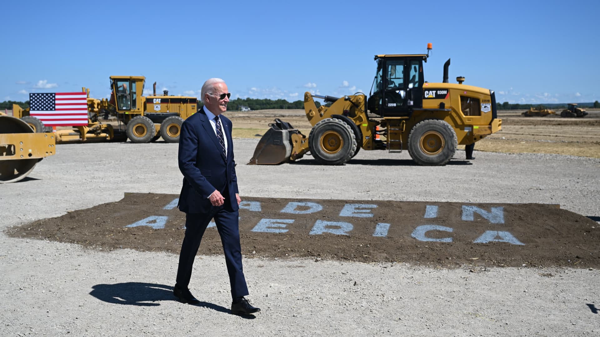
With Taiwan Semiconductor (NYSE:TSM) set to boost its investment in a massive new chip foundry in Arizona, several big-name tech executives are set to join President Joe Biden during a visit to the facility on Tuesday.

Among those heading to Taiwan Semi's (TSM) plant near Phoenix are some of the heavyweight of the semiconductor market, including Apple (NASDAQ:AAPL) Chief Executive Tim Cook, Nvidia (NASDAQ:NVDA) CEO and founder Jensen Huang and Micron Technology (NASDAQ:MU) CEO Sanjay Mehrotra. The three will be joined by Taiwan Semi (TSM) founder Morris Chang.

The White House said President Biden and the tech executives will hold a "tool-in" ceremony that involves a ceremonial moving of equipment to the production area of the Taiwan Semi (TSM) plant/

Taiwan Semi (TSM), which is the world's biggest chip foundry, said it will build a second chipmaking plant in Arizona, which will boost its investments in the state to $40B after initially saying it will put $12B into its first plant in the state.

The involvement of Apple's (AAPL) Cook and Nvidia's (NVDA) Huang at Tuesday's event shouldn't be a surprise, as reports on Monday said the two CEO's companies will be among the first customers to source chips made at the Taiwan Semi facilities.
 
I had suspected the site would be bigger than $12 billion but $40 billion is seriously massive. This is a positive for the industry any way you put it. Does dent Pat's narrative that Intel should be the vendor of choice of U.S government contracts when TSMC is expanding at should a torrid pace in North America.
I doubt the DOD was ever going to leave TSMC in it's entirety. Of course Intel will probably have more US foundry capacity long term, and the added benefit of everything from R&D to packaging being done in the US is good for extremely discrete projects. But no doubt expanded US presence will make TSMC more competitive for DOD contracts.
 
No clue why Sanjay Mehrotra is going there but sure. More logic is only good for the memory folks.
I remember reading this article from a while back. It might be a clue, other than Mehrotra being there because it was the place to be.

 
If TSMC was doing nothing, IMO Intel's foundry and expansion strategy would still be risky. I think Intel needs a customer-first attitude that I've never seen or heard about to be successful as a foundry. Perhaps the people from Tower will help change Intel culture in that regard.

Given all of the fab investments being announced, it does seem like there could be quite a glut of capacity in about five years for N to N-2 nodes.
TSMC management has been very diligent with capacity build out and in addition to pre payments I'm sure they will be more then fine. TSMC's C-Suite inspires a lot of confidence (my opinion).
 
TSMC management has been very diligent with capacity build out and in addition to pre payments I'm sure they will be more then fine. TSMC's C-Suite inspires a lot of confidence (my opinion).
The problem would be Samsung and Intel undercutting them. With the slowdown even if Intel and Samsung can’t catch up, the older stuff will be more competitive than you would otherwise guess given its age. Obviously this won’t sink TSMC. However it could and likely will hurt their margins.
 
The problem would be Samsung and Intel undercutting them. With the slowdown even if Intel and Samsung can’t catch up, the older stuff will be more competitive than you would otherwise guess given its age. Obviously this won’t sink TSMC. However it could and likely will hurt their margins.
If Intel wants to go this route I believe TSMC would be happy to return the favour many times over. TSMC has substantially better gross and operating margins than Intel, with Intel even losing money for a quarter or two this year as is. TSMC could easily go nuclear on Intel and aggressively undercut them (Intel) back. Basically it would be an arms race in which Intel would just lose even harder then they are now if they poked the TSMC bear. As for Samsung I'm not entirely sure as they really don't break down foundry financials very transparently but I would imagine getting into a pricing war with TSMC would be a poor idea as well especially since so much of their revenue is in the vulnerable memory space. TSMC for its part should seek to build and expand their existing partnership with Micron as much as possible to really go help undercut Samsungs semi devisions golden goose (the memory business). All of this is my opinion of course.
 
If Intel wants to go this route I believe TSMC would be happy to return the favour many times over. TSMC has substantially better gross and operating margins than Intel, with Intel even losing money for a quarter or two this year as is. TSMC could easily go nuclear on Intel and aggressively undercut them (Intel) back. Basically it would be an arms race in which Intel would just lose even harder then they are now if they poked the TSMC bear. As for Samsung I'm not entirely sure as they really don't break down foundry financials very transparently but I would imagine getting into a pricing war with TSMC would be a poor idea as well especially since so much of their revenue is in the vulnerable memory space. TSMC for its part should seek to build and expand their existing partnership with Micron as much as possible to really go help undercut Samsungs semi devisions golden goose (the memory business). All of this is my opinion of course.
Competition causing TSMC to lower their margins was my whole point. TSMC is incumbent and people won't switch to intel unless it is some combination of being easy to design for, comparable or better PPA, or being cheaper. Given that 18A uses single patterning EUV, and that i4 has a lower mask count than i7 I would be shocked if Intel's cost structure didn't improve over the coming years (to say nothing of the narrowing gap between the two foundries). With TSMC's high margin intel will probably be able to charge a more modest margin while they try to build up a fleshed out design ecosystem.

Like you said TSMC could lower margins to burry intel; and your right they could. But they wouldn't want to do that. Their margin is what sustains their growth engine and attracts investors. I would have to assume they will lower their margins slightly by virtue of having to compete with other foundries (and their own older processes). If memory serves someone on this forum said that TSMC trailing edge prices fell not long after intel 16 was announced for IFS.

As for Samsung they have always and will always undercut TSMC. From what I hear Samsung's fabs run a very tight ship. Combine this with their unimaginable scale, the logic side being subsidized by the memory side, and foundry just existing to get some extra money from the nodes they developed for their embedded processors and SOCs; and you get a company that can sustainably charge the bare minimum.
 
Last edited:
I doubt the DOD was ever going to leave TSMC in it's entirety. Of course Intel will probably have more US foundry capacity long term, and the added benefit of everything from R&D to packaging being done in the US is good for extremely discrete projects. But no doubt expanded US presence will make TSMC more competitive for DOD contracts.

Intel's SAT is largely outside of USA.
 
I doubt the DOD was ever going to leave TSMC in it's entirety. Of course Intel will probably have more US foundry capacity long term, and the added benefit of everything from R&D to packaging being done in the US is good for extremely discrete projects. But no doubt expanded US presence will make TSMC more competitive for DOD contracts.

DOD contacts or not, you can't develop a modern chip today without decent IP ecosystem, or you have to work with 10 years old macros.

This is the paradox why Intel HAS to manufacture Atom CPUs at TSMC. They were a hasty rushed "napkin product" to plug the low-end to deny it to AMD, and ARM stuff.

They had to use off-the shelf IP, since they didn't want to spend their Core X design team time dealing with grunt work reinveting the bicycle for an insignificant SKU. And the only decent IP, and capacity was at TSMC. The rest is history.

Now, there is simply not much 3rd party macros on the market for sub <40nm for any fab other than TSMC.
 
I had suspected the site would be bigger than $12 billion but $40 billion is seriously massive. This is a positive for the industry any way you put it. Does dent Pat's narrative that Intel should be the vendor of choice of U.S government contracts when TSMC is expanding at such a torrid pace in North America.

It would be if it was 300k WPM, but this is a WPY. Still nowhere near a megafab scale.
 
Intel's SAT is largely outside of USA.
Isn't AZ the biggest fab intel has? My understanding is Israel is similar in size, with OR and IR being similar in size. It is also my understanding that Germany is supposed to be kind of small (especially in comparison to what a fully built out OH will look like). Packaging is something where it is mostly outside the US. But the newly repurposed Fab11X gives Intel something for DOD contracts, no?
 
Competition causing TSMC to lower their margins was my whole point. TSMC is incumbent and people won't switch to intel unless it is some combination of being easy to design for, comparable or better PPA, or being cheaper. Given that 18A uses single patterning EUV, and that i4 has a lower mask count than i7 I would be shocked if Intel's cost structure didn't improve over the coming years (to say nothing of the narrowing gap between the two foundries). With TSMC's high margin intel will probably be able to charge a more modest margin while they try to build up a fleshed out design ecosystem.

TSMC doubling the capacity in USA is really bad news for Intel actually. The faster they can start production, the quicker they can eat that juicy $50B subsidy package, and leave nothing of that for Intel.

I imagine Intel will have to DOWNGRADE their CURRENT few years old process to make 18A mass market viable.

So Intel's aspiration to becoming a fab will likely only lead to it being a very expensive 3rd, or maybe 2nd tier fab, and not 1st.
 
Isn't AZ the biggest fab intel has? My understanding is Israel is similar in size, with OR and IR being similar in size. It is also my understanding that Germany is supposed to be kind of small (especially in comparison to what a fully built out OH will look like). Packaging is something where it is mostly outside the US. But the newly repurposed Fab11X gives Intel something for DOD contracts, no?

Intel can make super-duper overpriced DOD FPGAs already, and pay the few remaining US OSATs a king's ransom to work with such low volume.

Too bad, defence been preferring Xilinx over Altera for decades, with original reason for that being the lower price, off-the-shelf availability of Xilinx, and less of an Ivory tower attitude from them.
 
I imagine Intel will have to DOWNGRADE their CURRENT few years old process to make 18A mass market viable.

So Intel's aspiration to becoming a fab will likely only lead to it being a very expensive 3rd, or maybe 2nd tier fab, and not 1st.
What do you even mean by this? 10nm is in about as good of a state as you could ask given it's inherent cost structure disadvantages. Per intel, intel 4 is already hitting yields for HVM (and Oregon has plenty of EUV tools for the task). Hopefully the design side is getting their execution on track.
 
Back
Top