user nl
Well-known member
https://tspasemiconductor.substack.com/p/ofc-2026-summary-how-silicon-photonics
In the AI era, the bottleneck is no longer just within the chip itself—
it lies between chips, between racks, and between switches and accelerators.
The real question is whether we can connect the entire system—
with acceptable power consumption, manageable latency, and manufacturable packaging.
This is the essence of OFC 2026.
Optical communications is no longer just a showcase for modules, lasers, DSPs, or switching components. It has officially become a system-level battlefield for AI infrastructure.
From NVIDIA’s definition of the AI Factory, to Meta’s 90-million-hour reliability validation for CPO; from Broadcom pushing CPO toward commercial maturity, to Intel driving OCI into the package; from ST and Samsung bringing silicon photonics onto 300mm platforms, to FormFactor and GF/Cadence tackling testing and EDA—two of the least glamorous yet most critical barriers to scale—
the entire industry is, in fact, answering the same question:
As AI clusters scale to 100K, 500K, or even 1 million GPUs, what should the future data center interconnect actually look like?
It was an open debate about the “system physics” of the AI era.
Because when:
The future competition is not just about who has more GPUs—
but who can assemble those GPUs into a working AI factory with:
From raw bandwidth → to architectural partitioning between scale-up and scale-out
But as model sizes and data flows explode, that assumption is breaking down.
OpenAI’s framing at the conference was particularly direct: inference token growth is no longer linear but expanding by orders of magnitude, which implies that each new generation of infrastructure must simultaneously deliver roughly 2× improvements in bandwidth density while continuously reducing I/O power; otherwise, the economics of the AI factory will deteriorate rapidly.
Source: epoch.ai
SEMIVISION @_@ is a reader-supported publication. To receive new posts and support my work, consider becoming a free or paid subscriber.
Subscribe
OFC 2026: The Moment AI Infrastructure Moved Beyond the Chip
If the dominant theme of the semiconductor industry over the past decade was process scaling, then what truly stood out at OFC 2026 was a deeper and far more structural shift:In the AI era, the bottleneck is no longer just within the chip itself—
it lies between chips, between racks, and between switches and accelerators.
The real question is whether we can connect the entire system—
with acceptable power consumption, manageable latency, and manufacturable packaging.
This is the essence of OFC 2026.

Optical communications is no longer just a showcase for modules, lasers, DSPs, or switching components. It has officially become a system-level battlefield for AI infrastructure.
From NVIDIA’s definition of the AI Factory, to Meta’s 90-million-hour reliability validation for CPO; from Broadcom pushing CPO toward commercial maturity, to Intel driving OCI into the package; from ST and Samsung bringing silicon photonics onto 300mm platforms, to FormFactor and GF/Cadence tackling testing and EDA—two of the least glamorous yet most critical barriers to scale—
the entire industry is, in fact, answering the same question:
As AI clusters scale to 100K, 500K, or even 1 million GPUs, what should the future data center interconnect actually look like?
OFC 2026: Not a Telecom Show, but a Debate on “System Physics” in the AI Era
In this context, OFC 2026 was not merely an optical communications conference.It was an open debate about the “system physics” of the AI era.
Because when:
- Rack-level power scales from 120 kW to 600 kW,
- A single AI factory demands hundreds of megawatts,
- Both training and inference begin treating networking as a first-class resource, interconnect is no longer a supporting role—it becomes core infrastructure that determines whether compute can be monetized.
What this really implies is:“The data center is a computer, and the network defines its boundaries.”
The future competition is not just about who has more GPUs—
but who can assemble those GPUs into a working AI factory with:
- The lowest pJ/bit,
- The smallest failure domain (blast radius),
- The highest serviceability.
The Real Bottleneck of AI Factories: Not Compute, but Whether Interconnect Can Keep Up with Agentic Scaling
Historically, discussions around AI infrastructure have focused on GPUs, HBM, advanced packaging, and process nodes, but at OFC 2026 one signal became unmistakably clear: the performance scaling of compute cores is now outpacing the scaling of I/O and networking, fundamentally shifting the bottleneck. The key question is no longer whether a single chip is fast enough, but whether the entire cluster can operate as if it were a single chip.From Bandwidth to Architecture: Scale-Up vs. Scale-Out
This is why companies across the spectrum— OpenAI, Microsoft, AMD, NVIDIA, and Broadcom— are shifting the discussion:From raw bandwidth → to architectural partitioning between scale-up and scale-out
- Scale-up: ultra-low latency, high synchronization efficiency between accelerators
- Scale-out: throughput, elasticity, and scalability across racks and clusters
But as model sizes and data flows explode, that assumption is breaking down.
OpenAI’s framing at the conference was particularly direct: inference token growth is no longer linear but expanding by orders of magnitude, which implies that each new generation of infrastructure must simultaneously deliver roughly 2× improvements in bandwidth density while continuously reducing I/O power; otherwise, the economics of the AI factory will deteriorate rapidly.

Source: epoch.ai
SEMIVISION @_@ is a reader-supported publication. To receive new posts and support my work, consider becoming a free or paid subscriber.
Subscribe
Below we will share:
- Silicon Photonics Has Finally Entered the True 300 mm Era—But the Bottleneck Is No Longer Just the Device
- 1.6T Is No Longer the Future — The Real Battlefield Lies in 3.2T and Beyond 400G/lane
- From Pluggables to CPO to OCI: The Interconnect Boundary Keeps Moving Closer to the Chip
- Meta Has Answered the Hardest Question Around CPO: Reliability
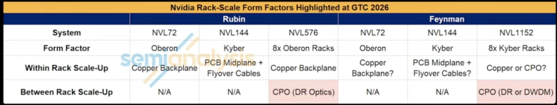
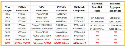
- NVIDIA, Lightmatter, and Broadcom Represent Three Different Futures: High-Density Microrings, In-Package DWDM, and System-Level CPO
- The Real Implication for Taiwan and the Supply Chain: The Center of Value in Optical Interconnects Is Shifting from Modules to Platforms and Packaging