Intel has attracted plenty of chatter over the past few weeks, with talk that Apple could come crawling back for some M-series work, but now it appears that iPhone chips…

Intel has attracted plenty of chatter over the past few weeks, with talk that Apple could come crawling back for some M-series work, but now it appears that iPhone chips on Chipzilla’s fanciest nodes are a non-starter.
In recent weeks, GF Securities and DigiTimes have claimed Apple might use Chipzilla’s 18A-P process for its lowest-end M-series parts in 2027. The same reports floated the possibility of non-Pro iPhone chips in 2028.
GF Securities also said Job’s Mob’s bespoke ASIC, expected in 2028, would use Chipzilla’s EMIB packaging. That is the sort of detail that makes rumours sound “real” while still being completely free of consequences.
There has been noise that Job’s Mob signed an NDA with Intel and pulled PDK samples for 18A-P to evaluate. Chipzilla’s 18A-P is intended to be its first node supporting Foveros Direct 3D hybrid bonding, enabling chiplets stacking via TSVs.
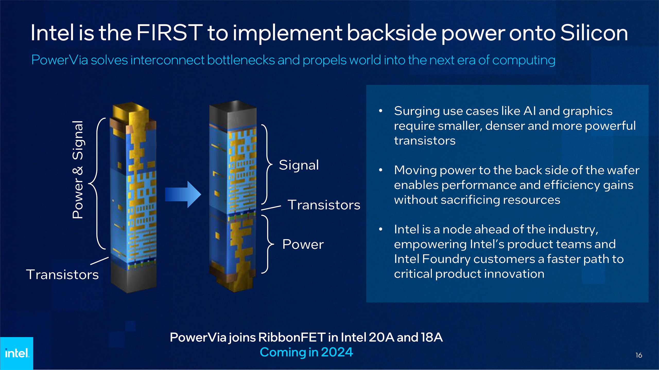
Now, a bunch of industry insiders on the SemiWiki forum have poured cold water on Intel’s manufacturing of iPhone chips. The core gripe is Chipzilla’s decision to go all-in on Backside Power Delivery for its 18A and 14A nodes.
Unlike TSMC, which offers some nodes with BSPD and others without it, Chipzilla has pushed BSPD across its bleeding-edge stack. That leaves it without an easy “same node, less drama” option when a customer prioritises thermals over bragging rights.
BSPD can boost performance because the chip is powered through shorter, thicker metal paths on the backside, cutting voltage drop and helping to stabilise frequencies. It also frees up front-side routing, which can lift transistor density or reduce congestion.
For mobile silicon, insiders reckon the performance bump is small. The trade-off is a worse self-heating effect, which increases cooling requirements in places phones would rather avoid.
SemiWiki forum, commenter IanD said: “kept around 20C cooler with BSPD for the same die temperature in hotspots (because vertical heat spreading is bad but lateral is even worse now there’s no thick silicon substrate), and that’s simply impossible in many use cases which rely on air cooling or have a maximum allowable case temperature.”
X, commentator Jukan said there is “zero chance” that Chipzilla can manufacture Job’s Mob iPhone chips anytime soon, although he thought that M-series parts might still be on the table.
Intel has attracted plenty of chatter over the past few weeks, with talk that Apple could come crawling back for some M-series work, but now it appears that iPhone chips on Chipzilla’s fanciest nodes are a non-starter.
In recent weeks, GF Securities and DigiTimes have claimed Apple might use Chipzilla’s 18A-P process for its lowest-end M-series parts in 2027. The same reports floated the possibility of non-Pro iPhone chips in 2028.
GF Securities also said Job’s Mob’s bespoke ASIC, expected in 2028, would use Chipzilla’s EMIB packaging. That is the sort of detail that makes rumours sound “real” while still being completely free of consequences.
There has been noise that Job’s Mob signed an NDA with Intel and pulled PDK samples for 18A-P to evaluate. Chipzilla’s 18A-P is intended to be its first node supporting Foveros Direct 3D hybrid bonding, enabling chiplets stacking via TSVs.
Now, a bunch of industry insiders on the SemiWiki forum have poured cold water on Intel’s manufacturing of iPhone chips. The core gripe is Chipzilla’s decision to go all-in on Backside Power Delivery for its 18A and 14A nodes.
Unlike TSMC, which offers some nodes with BSPD and others without it, Chipzilla has pushed BSPD across its bleeding-edge stack. That leaves it without an easy “same node, less drama” option when a customer prioritises thermals over bragging rights.
BSPD can boost performance because the chip is powered through shorter, thicker metal paths on the backside, cutting voltage drop and helping to stabilise frequencies. It also frees up front-side routing, which can lift transistor density or reduce congestion.
For mobile silicon, insiders reckon the performance bump is small. The trade-off is a worse self-heating effect, which increases cooling requirements in places phones would rather avoid.
SemiWiki forum, commenter IanD said: “kept around 20C cooler with BSPD for the same die temperature in hotspots (because vertical heat spreading is bad but lateral is even worse now there’s no thick silicon substrate), and that’s simply impossible in many use cases which rely on air cooling or have a maximum allowable case temperature.”
X, commentator Jukan said there is “zero chance” that Chipzilla can manufacture Job’s Mob iPhone chips anytime soon, although he thought that M-series parts might still be on the table.

")