Array
(
    [content] => 
    [params] => Array
        (
            [0] => /forum/threads/tachyum-unveils-2nm-prodigy-with-21x-higher-ai-rack-performance-than-the-nvidia-rubin-ultra.24007/
        )

    [addOns] => Array
        (
            [DL6/MLTP] => 13
            [Hampel/TimeZoneDebug] => 1000070
            [SV/ChangePostDate] => 2010200
            [SemiWiki/Newsletter] => 1000010
            [SemiWiki/WPMenu] => 1000010
            [SemiWiki/XPressExtend] => 1000010
            [ThemeHouse/XLink] => 1000970
            [ThemeHouse/XPress] => 1010570
            [XF] => 2030770
            [XFI] => 1060170
        )

    [wordpress] => /var/www/html
)

Tachyum Unveils 2nm Prodigy with 21x Higher AI Rack Performance than the Nvidia Rubin Ultra

Daniel Nenni

Admin
Staff member
Tachyum Unveils 2nm Prodigy with 21x Higher AI Rack Performance than the Nvidia Rubin Ultra


LAS VEGAS, November 12, 2025 –Tachyum® today announced details and specifications for its 2nm Prodigy® Universal Processor, which will enable AI models with parameters many orders of magnitude larger than those of any existing solution at a fraction of the cost.

Prodigy Ultimate provides up to 21.3x higher AI rack performance than Nvidia Rubin Ultra NVL576. Prodigy Premium provides up to 25.8x higher AI rack performance than Vera Rubin 144. Technical details of the 2nm Prodigy, the first ever chip to exceed 1,000 PFLOPs on inference, will be published within a week. Nvidia Rubin delivers 50 PFLOPs.

The global competition in AI continues to accelerate, with China and the United States leading the race. Current AI models demonstrate massive computational scales — for instance, ChatGPT 4 features approximately 1.8 trillion parameters, while human brains contain an estimated 150 trillion synapses. Emerging systems such as BaGauLu reach 174 trillion parameters, but the ultimate breakthrough is expected to come from models trained on the collective knowledge of humanity, exceeding 100 000 000 trillion (1020) parameters. Traditional large-scale AI solutions could cost over $8 trillion and require more than 276 gigawatts of power. In contrast, the Tachyum solution is projected to achieve comparable capabilities at an estimated cost of $78 billion and a power requirement of just 1 gigawatt — making it accessible to multiple companies and nations.
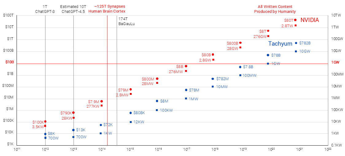


AI Revolution Chart


In addition to open-sourcing all software, Tachyum is making its memory technology available, using standard components, allowing 10x increase of DIMM-based memory bandwidth available for licensing by memory or processor companies, including JEDEC adoption to achieve high adoption and low cost. In 2023, Tachyum announced licensable Tachyum AI (TAI) data types, and its Tachyum Processing Unit (TPU) core is available for licensing. Tachyum is in the process of making the Instruction Set Architecture (ISA) open.

Tachyum has continually upgraded its Prodigy design to address ever-changing requirements in server, AI and HPC markets with up to 5x integer performance, up to 16x higher AI performance, 8x DRAM bandwidth, 4x chip-to-chip and I/O bandwidth, 4x scalability by supporting 16 sockets, and 2x power efficiency, with lower cost per core.

The Prodigy chip was upgraded to 2nm to significantly reduce power consumption. Reducing chiplet die size improves cost despite expensive 2nm wafers. Each chiplet in the Prodigy package integrates 256 high-performance custom 64-bit cores. The power consumption reduction is critical, as multiple chiplets occupy a single package. Backed by a recent $220 million investment, the 2nm Prodigy is being readied for tape-out.

Multiple Prodigy SKUs cover a wide range of performance and applications, including big AI, exascale supercomputing, HPC, digital currency, cloud/hyperscale, big data analytics, and databases. Prodigy Ultimate integrates 1,024 high-performance cores, 24 DDR5 17.6GT/s memory controllers and 128 PCIE 7.0 lanes. The Prodigy Premium comes with 16 DRAM channels, and 512 to 128 cores scalable to 16 socket systems. Entry-level Prodigy comes with 8 or 4 DRAM controllers and 128 to 32 cores.

Prodigy features, scalability, and price segmentation ensure rapid market penetration. Tachyum provides out-of-the-box native system software, operating systems, compilers, libraries, many applications, and AI infrastructure frameworks. It also allows running unmodified Intel/AMD x86 binaries and mixing them with native applications. This ensures that Tachyum systems can be operational by customers from day one.

“With tape-out funding now secured after a long wait, the world’s first Universal Processor can proceed to production, designed to overcome the inherent limitations of today’s data centers,” said Dr. Radoslav Danilak, founder and CEO of Tachyum. “The distinct markets addressed by Prodigy are the AI, server, and HPC markets, requiring fast and efficient chips. Tachyum’s Prodigy Premium and Ultimate will supercharge workloads with superior performance at a lower cost than any other solution on the market.”

The Prodigy Universal Processor delivers orders of magnitude higher AI performance, 3x the performance of the best x86 processors, and 6x HPC performance of the fastest GPGPU. Eliminating the need for expensive dedicated AI hardware and dramatically increasing server utilization, Prodigy reduces data center CAPEX and OPEX significantly while delivering unprecedented performance, power, and economics.

Those interested in reading the full specifications for Tachyum’s latest Prodigy Universal Processor architecture can download the solutions brief.

Tachyum is transforming the economics of AI, HPC, public and private cloud with the world’s first Universal Processor Prodigy unifying the functionality of a CPU, an HPC GPGPU, and AI accelerators to deliver industry-leading performance, cost and power efficiency. Tachyum has offices in the United States, Slovakia, Taiwan and the Czech Republic. For more information, visit https://www.tachyum.com/.
 
Impressive chip. From what I heard it is TSMC N2 but I'm wondering why they did not mention it? It says they have an office in Taiwan.......
they said they are upgrading it to 2nm. they also said "with tape-out funding resolved, ..." which indicates not taped out yet? do we know when any independent BM can be run on their real chips?
 
Universal Processors? They look like very high clock frequency CPUs to me, with vector units and some special instructions. I've never heard of these guys before. Does anyone know if they've ever produced any actual chips?
 
Last edited:
Universal Processors? They look like very high clock frequency CPUs to me, with vector units and some special instructions. I've never heard of these guys before. Does anyone know if they've ever produced any actual chips?

These guys sound a lot like Intel once did - just throw a bunch of parallel processors with fancy vector / tensor units at the AI problem. I'm seeing too many "chip breakthroughs" that ignore the whole structure of transformer-based models, and simple throw brute force vector/tensor units into the fray, instead of a application-targeted architecture. I'm only going to believe the companied who talk in terms of transformer model specifics - attention, multi-headed self attention mechanisms, KV caches and management, smart quantization (FP4 anyone), disaggregation of profile/context and decode, and point to point communication between compute units. So much of the magic is going to be in hardware architecture and the software to manage it at scale with massive parallelism. The brute force number claims are a bit ridiculous without the important discussions about the AI system architecture.

 
These guys sound a lot like Intel once did - just throw a bunch of parallel processors with fancy vector / tensor units at the AI problem.
Yup. Larrabee. :)
I'm seeing too many "chip breakthroughs" that ignore the whole structure of transformer-based models, and simple throw brute force vector/tensor units into the fray, instead of a application-targeted architecture. I'm only going to believe the companied who talk in terms of transformer model specifics - attention, multi-headed self attention mechanisms, KV caches and management, smart quantization (FP4 anyone), disaggregation of profile/context and decode, and point to point communication between compute units. So much of the magic is going to be in hardware architecture and the software to manage it at scale with massive parallelism. The brute force number claims are a bit ridiculous without the important discussions about the AI system architecture.

I agree. This is why Google insists on developing multiple generations of TPUs and their own software stack. They are the inventors of the attention concept, so they know what they need to do to accelerate it.

For a short time I was associated with a couple of flash storage projects, not by choice, by assignment. Several of the long-term flash storage people on the projects knew Rado from Skyera. Apparently he's a very interesting individual. :rolleyes:
 
I'm connected to the CEO on LinkedIn, I requested an interview. So many questions...
Rado is a good guy, very smart. we met on High performance SSDs back in the day. (Sandforce and then when I worked with HGST)

I expect it to be very low volume niche. But let me know how the interview goes

What is the mask set cost of a N2 product these days? Approximate
 
Original specifications were interesting but still somewhat believable. Lot of vliw cores at very high frequency which was achieved by giving up out-of-order execution. It made sense specially back then when x86 did not had wide vector units and most of core were scheduling resources. So basic assumption was that Tachyum will replace most of non-execution blocks with vector units while maintaining high frequency and low power..

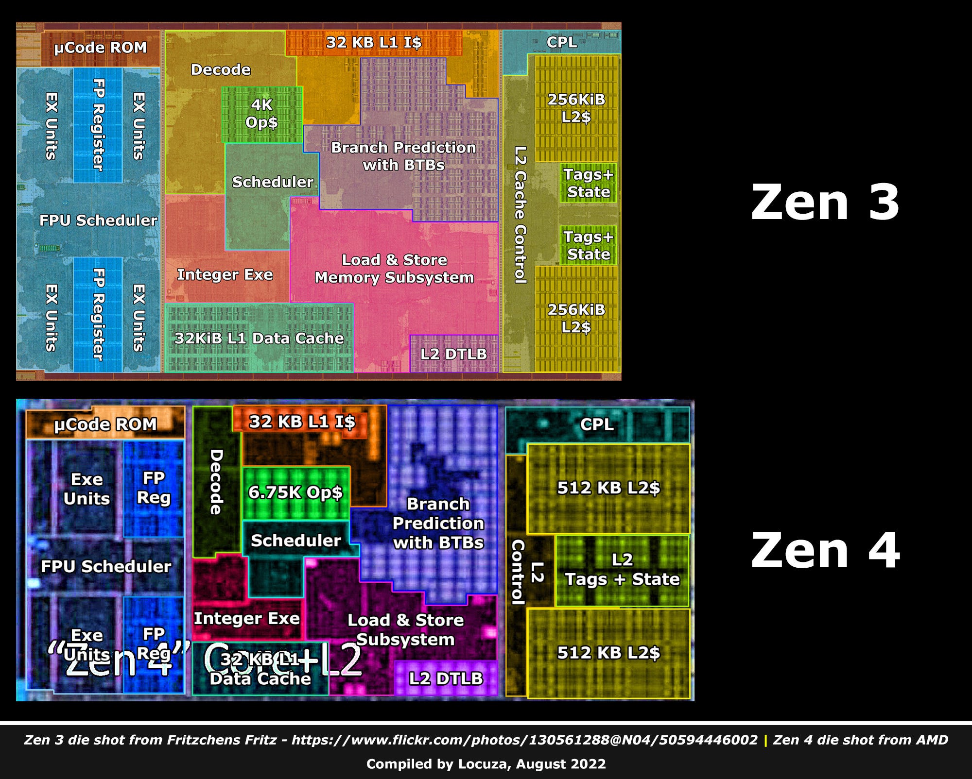
https%3A%2F%2Fbucketeer-e05bbc84-baa3-437e-9518-adb32be77984.s3.amazonaws.com%2Fpublic%2Fimages%2F553cf263-224b-475d-8949-f97d2d13a187_2000x1604.jpeg


Now they claim to support ooo without giving up other aspects, and it triggers scam alarms even in people which previously believed that Tachyum can deliver.
Screenshot 2025-11-14 094130.jpg
 
Rado is a good guy, very smart. we met on High performance SSDs back in the day. (Sandforce and then when I worked with HGST)

I expect it to be very low volume niche. But let me know how the interview goes

What is the mask set cost of a N2 product these days? Approximate
An N2 mask set is around $30M, but this is usually dwarfed by the cost of the tools and software and people needed to design and verify the chip...
 
Original specifications were interesting but still somewhat believable. Lot of vliw cores at very high frequency which was achieved by giving up out-of-order execution. It made sense specially back then when x86 did not had wide vector units and most of core were scheduling resources. So basic assumption was that Tachyum will replace most of non-execution blocks with vector units while maintaining high frequency and low power..
When I was reading about their early design, I never saw references to VLIW. Did you?
 
Such massive performance improvement compared to Nvidia from what is basically a customised CPU array with vector extensions seems *very* unlikely, it's not exactly a new concept.

The only way I can see of getting such a huge leap in power/efficiency is a radically new architecture, for example an application-specific data-driven/dynamically reconfigurable dataflow engine merged with RAM into an ultrawideband/low-latency network -- just an example, not saying this can deliver what is suggested!
 
What is the mask set cost of a N2 product these days? Approximate

From what I have heard it is closer to $25M than $30M. N2 has a reduced mask set versus N3. TSMC is trying to cut costs for sure.

We should hear more about this at IEDM next month. I hope to see you there again. Let's grab coffee.
 
An N2 mask set is around $30M, but this is usually dwarfed by the cost of the tools and software and people needed to design and verify the chip...

Hyperscalers are spending huge amounts of money on design versus the fabless chip or the ASIC design companies. I did a project with Google and they wrote some very big EDA/IP checks. Companies like Qualcomm and Broadcom are penny pinchers in comparison. If you want to know what the baseline cost of a design for a complex SoC is ask Alchip. They are doing N3 and N2 chips and have the best margins in the services business.
 
From what I have heard it is closer to $25M than $30M. N2 has a reduced mask set versus N3. TSMC is trying to cut costs for sure.

We should hear more about this at IEDM next month. I hope to see you there again. Let's grab coffee.
I don't know what you've heard or from who, only what we're expecting to pay for N2P next year -- and last I heard it was around $30M... :-(

(maybe massive customers like Apple or AMD or Nvivia are paying less? maybe TSMC have recently reduced mask prices?)

Also not sure where your "reduced mask set" comes from, given the introduction of GAA -- last time I counted up there were more masks in N2 than N3...
 
Last edited:
Back
Top