You are currently viewing SemiWiki as a guest which gives you limited access to the site. To view blog comments and experience other SemiWiki features you must be a registered member. Registration is fast, simple, and absolutely free so please, join our community today!
It is reported that Intel's next-generation client CPU flagship product Nova Lake-S has been taped out at TSMC's wafer fab in Taiwan. We previously speculated based on rumors that Intel will adopt its own internal 18A process and rely on TSMC's 2nm mass production technology. But according to SemiAccurate's report, Intel has taped out a computing module on TSMC's N2 process, which means that the computing module of Nova Lake-S will most likely use both 18A and TSMC's N2 processes. One possible reason for Intel's decision is that if the 18A process cannot be delivered, or if demand is expected to be too high and internal production capacity cannot be met, Intel is building a reliable backup plan. In any case, customers can expect the product to be delivered on time in the second half of 2026, but there may be some interesting solutions behind it.
As for the specific date, it will take several months from Tape-Out to the delivery of the final product. Currently, the chips completed by Tape-Out are undergoing power-on testing in Intel laboratories, running various tests to test the performance of the chips under multiple uses and check the correctness of their operation. Normally it takes a few weeks to a month to power on, and final mass production will begin a few months later. It will take another two to three months to manufacture and ship, which means that Nova Lake-S will most likely be released in the third quarter of 2026. It should be reminded that this CPU will integrate up to 52 cores (16 P cores, 32 E cores and 4 LPE cores), with an 8,800MT/s memory controller, as well as Xe3 Celestial for graphics rendering and Xe4 Druid for media and display tasks. This undoubtedly makes it an extremely attractive product, but due to its heterogeneous complexity, its manufacturing difficulty is also quite high.
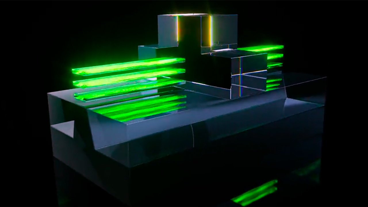
Also Known As: TSMC 2nm nodeDeveloper: Taiwan Semiconductor Manufacturing Company (TSMC)Node Class: Advanced logic semiconductor nodeTechnology Generation: 2 nanometer (2nm)Status (as of 2025): Risk production in progress; volume production expected in late 2025 or 2026 Overview The TSMC N2...
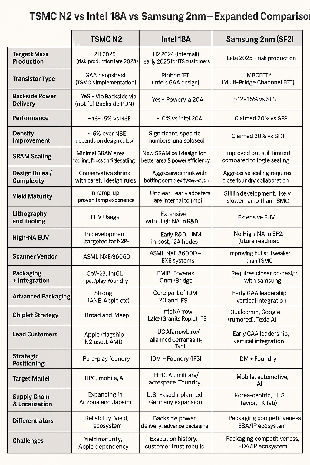
Category TSMC N2 Intel 18A Samsung 2nm (SF2) Target Mass Production 2H 2025 (risk production late 2024) H2 2024 (internal); early 2025 for IFS customers Late 2025 – risk production Transistor Type GAA nanosheet (TSMC’s implementation) RibbonFET (Intel's GAA design) MBCFET™ (Multi-Bridge Channel...
No real surprise here. At the BoA Technology Conference back on June 3rd Michelle Johnston-Holthaus said: "And so, I've been very public that come our next generation of product, Nova Lake, I'm using both TSMC and Intel Foundry. And I'm doing that because I think it allows me to deliver a more competitive product for our customers. And at the end of the day, the best product wins."
Also Known As: TSMC 2nm nodeDeveloper: Taiwan Semiconductor Manufacturing Company (TSMC)Node Class: Advanced logic semiconductor nodeTechnology Generation: 2 nanometer (2nm)Status (as of 2025): Risk production in progress; volume production expected in late 2025 or 2026 Overview The TSMC N2...
Category TSMC N2 Intel 18A Samsung 2nm (SF2) Target Mass Production 2H 2025 (risk production late 2024) H2 2024 (internal); early 2025 for IFS customers Late 2025 – risk production Transistor Type GAA nanosheet (TSMC’s implementation) RibbonFET (Intel's GAA design) MBCFET™ (Multi-Bridge Channel...
No real surprise here. At the BoA Technology Conference back on June 3rd Michelle Johnston-Holthaus said: "And so, I've been very public that come our next generation of product, Nova Lake, I'm using both TSMC and Intel Foundry. And I'm doing that because I think it allows me to deliver a more competitive product for our customers. And at the end of the day, the best product wins."
I remember you previously mentioned that Intel had no plans to use TSMC’s N2, but it now seems the strategy has shifted. Does this imply that Intel 18A may not be sufficiently mature, even for internal applications?
I remember you previously mentioned that Intel had no plans to use TSMC’s N2, but it now seems the strategy has shifted. Does this imply that Intel 18A may not be sufficiently mature, even for internal applications?
I said Intel had not signed a TSMC N2 agreement. That was more than a year ago. I was told that all but one TSMC N3 customer had signed an N2 agreement and that was Intel.
I had hoped Intel would use 18A for all internal designs but clearly that is not the case. I do think that TSMC N2 was plan B and now with the reorg and cutbacks it is a very good plan B.
I agree it's a good plan. Right now, Intel's biggest challenges lie in resolving its financial issues and boosting product competitiveness.
It also reminds me of a joke: using TSMC is like trying a drug—once you start, it's hard to quit.
Also Known As: TSMC 2nm nodeDeveloper: Taiwan Semiconductor Manufacturing Company (TSMC)Node Class: Advanced logic semiconductor nodeTechnology Generation: 2 nanometer (2nm)Status (as of 2025): Risk production in progress; volume production expected in late 2025 or 2026 Overview The TSMC N2...
Category TSMC N2 Intel 18A Samsung 2nm (SF2) Target Mass Production 2H 2025 (risk production late 2024) H2 2024 (internal); early 2025 for IFS customers Late 2025 – risk production Transistor Type GAA nanosheet (TSMC’s implementation) RibbonFET (Intel's GAA design) MBCFET™ (Multi-Bridge Channel...
Intel is creating back up plans and parallel plans for 18A products and maybe beyond. This will give them the flexibility needed to navigate the restructuring.
I would use 18 Months from Tapeout to Launch minimum.... even that might be a paper launch (products not on shelves).
We will see the product roadmap change before Nova lake gets launched.


")