Array
(
    [content] => 
    [params] => Array
        (
            [0] => /forum/threads/samsung-demonstrates-3gae-gate-all-around-mbcfets-at-isscc-2021.13889/
        )

    [addOns] => Array
        (
            [DL6/MLTP] => 13
            [Hampel/TimeZoneDebug] => 1000070
            [SV/ChangePostDate] => 2010200
            [SemiWiki/Newsletter] => 1000010
            [SemiWiki/WPMenu] => 1000010
            [SemiWiki/XPressExtend] => 1000010
            [ThemeHouse/XLink] => 1000970
            [ThemeHouse/XPress] => 1010570
            [XF] => 2021770
            [XFI] => 1050270
        )

    [wordpress] => /var/www/html
)

Samsung demonstrates 3GAE Gate-All-Around MBCFETs at ISSCC 2021


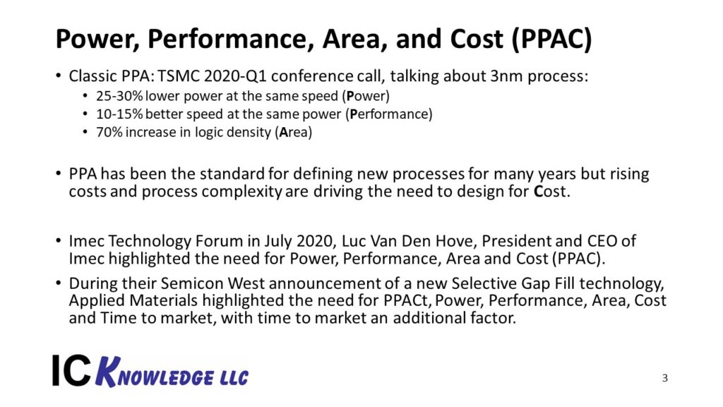
"In general, Samsung says that when compared to its 7LPP technology, its 3GAE node will enable an up to 30% performance improvement (at the same power and complexity), up to 50% lower power (at the same clocks and complexity), and an up to 80% higher transistor density (which includes a mix of logic and SRAM transistors)."
SRAM needs an underline here.
 
Scott Jones did a comparison here:


Spoiler alert: Samsung is behind TSMC in density @ 3nm (FinFET vs GAE).
 
Scott Jones did a comparison here:


Spoiler alert: Samsung is behind TSMC in density @ 3nm (FinFET vs GAE).

Not like just behind, but severely, 1.5 generations behind.
 
Well nanosheets are like fins lying on their side, so the horizontal width would not be as small as expected from the fin pitch anymore. I wonder if this causes some reverse scaling. Surely, for single fin locations.
 
Back
Top