Array
(
    [content] => 
    [params] => Array
        (
            [0] => /forum/threads/intel-14a-pitches-rumour.25322/
        )

    [addOns] => Array
        (
            [DL6/MLTP] => 13
            [Hampel/TimeZoneDebug] => 1000070
            [SV/ChangePostDate] => 2010200
            [SemiWiki/EmailDomainReplace] => 1000010
            [SemiWiki/Newsletter] => 1000010
            [SemiWiki/WPMenu] => 1000010
            [SemiWiki/XPressExtend] => 1000010
            [ThemeHouse/XLink] => 1000970
            [ThemeHouse/XPress] => 1010570
            [XF] => 2031070
            [XFI] => 1060170
        )

    [wordpress] => /var/www/html
)

Intel 14A pitches Rumour

I asked Gemini to explain dual side. It sounds very ambitious if its true.

In the context of your notes on Intel’s manufacturing roadmap (Intel 14A and 14A2), the distinction between "backside power direct only" and "dual side" refers to how the chip delivers electricity to its billions of transistors.

To understand this, it helps to visualize the chip as a multi-layered sandwich. Traditionally, signals and power are both routed on the "front side" (the top of the silicon), which causes traffic congestion and energy loss.

1. BACKSIDE POWER DIRECT (14A)
In this approach, Intel moves the power delivery network (the grid that carries electricity) from the top of the chip to the bottom (the backside).

•The Benefit: By moving power to the bottom, the "front side" is left almost entirely free for signal routing. This reduces congestion, allows for faster processing, and significantly improves power efficiency by shortening the path electricity travels to reach the transistors.
•"Direct Only": This likely refers to a specialized implementation where the power is delivered directly from the backside to the transistors via nano-Through-Silicon Vias (nTSVs) without complex, multi-layered power routing on the backside itself.

2. DUAL SIDE (14A2)
"Dual side" implies a more sophisticated and flexible power and signal architecture. It suggests that the chip can utilize both the front and the backside for more than just power delivery.

•Increased Complexity: Instead of just using the backside as a "power highway," a dual-side architecture can use both sides of the silicon for power, signals, and even clock distribution.
•Efficiency Gains: This design allows for even higher transistor density and better thermal management. By balancing the "load" of signals and power across both sides of the wafer, designers can avoid bottlenecks that occur when trying to pack everything onto one surface.

COMPARISON SUMMARY
Backside Power Direct Only (14A)
Primary Goal: Move power grid to the backside to free up frontside space.

Dual Side (14A2)
Primary Goal: Optimize both sides for a mix of power and signal routing.

Backside Power Direct Only (14A)
Complexity: Lower; focuses on "power-only" backside transport.

Dual Side (14A2)
Complexity: Higher; enables co-optimization of signal and power on both sides.

Backside Power Direct Only (14A)
Main Advantage: Reduced IR drop (less power loss) and better signaling.

Dual Side (14A2)
Main Advantage: Maximum density and routing flexibility; further reduction in congestion.
 
28 nm pitch was hinted at in an SPIE paper last year.

There's no advantage for increasing NA from 0.33 to 0.55 for a 28 nm pitch. The image formation is the same (2-beam).

The larger beam's angle for 0.33 NA has a lower mask multilayer reflectivity vs. 0.55 NA, which would lead to a ~10% dose bump to compensate. Throughput change not much, still ~ 100-110 WPH. However, the depth of focus for the tip-to-tip space is reduced x 1/2.8 for 0.55 NA vs. 0.33 NA (inversely proportional to NA^2). The DoF loss is more serious, could entail using an extra cut mask exposure.
 
Last edited:
28 nm pitch was hinted at in an SPIE paper last year.

There's no advantage for increasing NA from 0.33 to 0.55 for a 28 nm pitch. The image formation is the same (2-beam).

The larger beam's angle for 0.33 NA has a lower mask multilayer reflectivity vs. 0.55 NA, which would lead to a ~10% dose bump to compensate. Throughput change not much, still ~ 100-110 WPH. However, the depth of focus for the tip-to-tip space is reduced x 1/2.8 for 0.55 NA vs. 0.33 NA (inversely proporational to NA^2). The DoF loss is more serious, could entail using an extra cut mask exposure.
M0 pitch in TSMC N2 is less than 24nm... ;-)
 
I recall TSMC already had 28 nm pitch M0 for N5P.
Indeed -- but my point was that in N2 TSMC *already* have a smaller M0 pitch than single-exposure high-NA can deliver, as you said: "No defect‑free process window is observed for Metal 0 logic PnR, for any High-NA EUV dose and focus even at the 24 nm pitch"

That would mean double-exposure is needed for high-NA just like with current EUV, which removes one of the advantages of high-NA (replacing double-exposure with single-exposure).

I also guess that the triple-exposure needed for some vias might go down to double-exposure with high-NA, but that's still only a 33% saving not 50%.

All of which must put a dent in the economics of high-NA, even if ASML could ship enough machines to keep up with the rapidly-rising AI-driven TSMC demand...
Indeed, this must have gone thru TSMC's thinking, perhaps Samsung too?
 
Indeed -- but my point was that in N2 TSMC *already* have a smaller M0 pitch than single-exposure high-NA can deliver, as you said: "No defect‑free process window is observed for Metal 0 logic PnR, for any High-NA EUV dose and focus even at the 24 nm pitch"

That would mean double-exposure is needed for high-NA just like with current EUV, which removes one of the advantages of high-NA (replacing double-exposure with single-exposure).

I also guess that the triple-exposure needed for some vias might go down to double-exposure with high-NA, but that's still only a 33% saving not 50%.

All of which must put a dent in the economics of high-NA, even if ASML could ship enough machines to keep up with the rapidly-rising AI-driven TSMC demand...
Intel says you don't need Double Patterning for 0.55NA 24nm pitch
1781785308026.jpeg
 
Intel had the "confidence", from earlier (see the source years).
I also note the data is 2-3 years old, in other words before anyone has any experience with trying to actually put high-NA into volume production.

It wouldn't be the first time that something that looked feasible in theory or in the lab turned out to be a yield/cost nightmare in production -- you'd have thought Intel would have learned this from their 10nm debacle, but maybe not... ;-)
 
Intel had the tool since 2024 and i doubt Intel is dumb enough to do 10nm again they won't survive another 10nm.
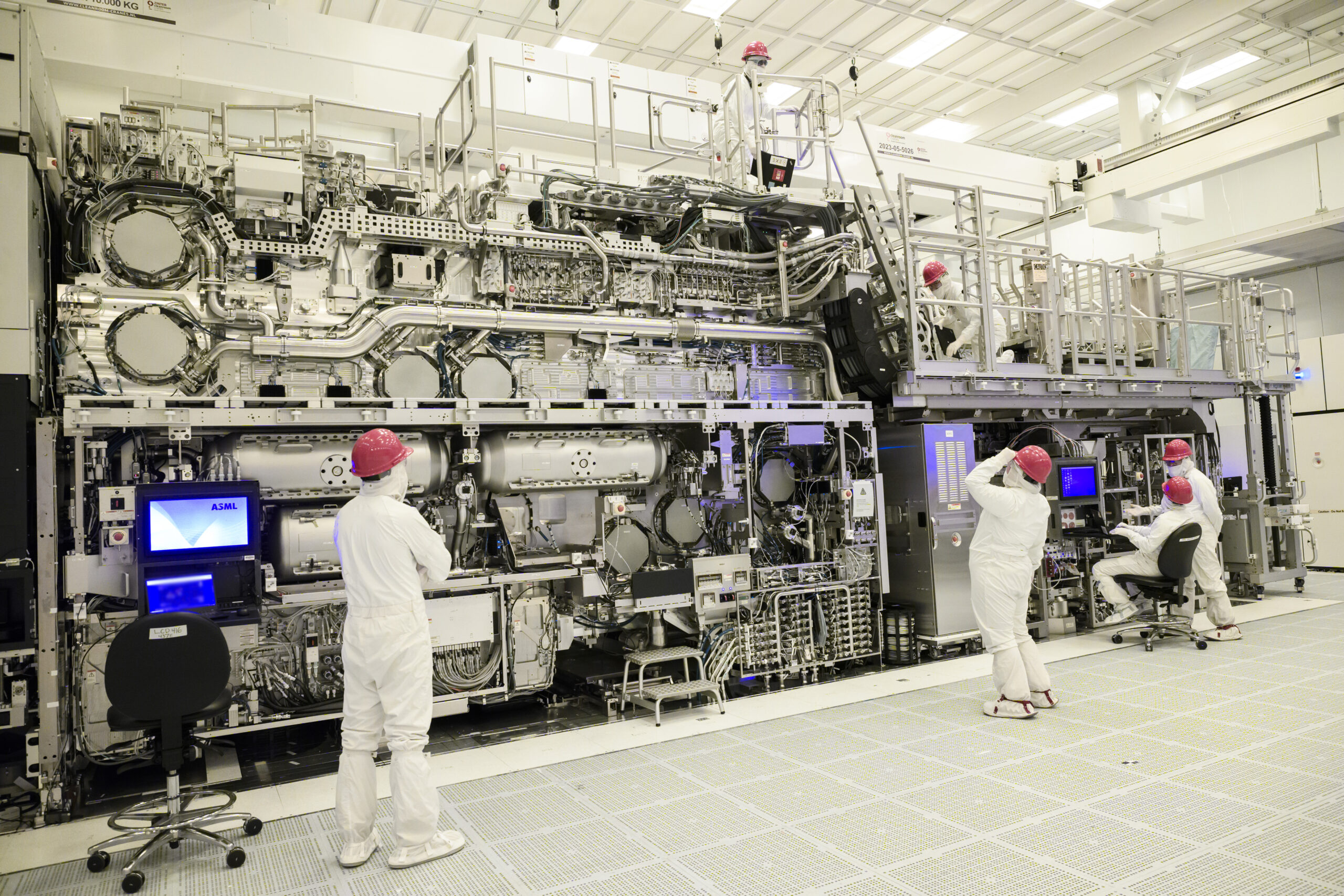
Intel have had a pre-production tool since 2024.

That's not the same as having multiple production tools running on a production line with high throughput/yield/availability.

The whole point of high-NA -- at least, in the near future -- is to avoid having to use multiple-patterned EUV, on the grounds that this saves money (fewer masks/steps), increases throughput, and reduces TAT.

All of which are *economic* factors, not technical ones. I don't think there's any doubt that high-NA will work, the question is whether it's better than 0.33NA in mass production -- especially in *very* big volumes, which TSMC need.

So it might be better for (lower-volume) Intel than 0.33NA -- given that Intel are less obsessive about cost and yield than TSMC -- while not making sense for TSMC, at least not for a few years until it's been improved (higher throughput), the cost has come down, and machine availability has improved.

That certainly seems to be TSMCs view, and as the dominant foundry who really knows about mass-production of bleeding-edge processes it's difficult to argue with that -- they'll introduce it later when it makes business sense.

Whether Intel are correct remains to be seen, the high-NA position is more favourable for them given their volumes and priorities -- and anyway they have to be seen to do something different to TSMC like "having the most advanced technology" early (see also BSPD), otherwise they're just a smaller-volume higher-priced follower without the TSMC ecosystem... ;-)
 
Intel says you don't need Double Patterning for 0.55NA 24nm pitch
View attachment 4747
So I went through the whole presentation just now. I am not sure why only one slide was posted originally by someone to make some judgments about High-NA vs. SALELE. This slide was actually in the middle of the talk, where the processes were compared to highlight that High-NA direct print would be simpler operation, particularly when moving from additive Cu to subtractive Ru metallization. After this, the High-NA direct print stochasticity was presented, using the 21 nm pitch case mostly. However, at 23 nm pitch, electrical defectivity was detected at the % level, so 24 nm would still be a definite high risk for High-NA (even ppb is bad enough), as the IMEC paper I quoted showed. They tried some process knobs to reduce roughness and resist bridges, but those ended up worsening resist breaks. Thus, they had to go to higher doses to reduce breaks, to the point of too high (new MOx resist needed).
 
So I went through the whole presentation just now. I am not sure why only one slide was posted originally by someone to make some judgments about High-NA vs. SALELE. This slide was actually in the middle of the talk, where the processes were compared to highlight that High-NA direct print would be simpler operation, particularly when moving from additive Cu to subtractive Ru metallization. After this, the High-NA direct print stochasticity was presented, using the 21 nm pitch case mostly. However, at 23 nm pitch, electrical defectivity was detected at the % level, so 24 nm would still be a definite high risk for High-NA (even ppb is bad enough), as the IMEC paper I quoted showed. They tried some process knobs to reduce roughness and resist bridges, but those ended up worsening resist breaks. Thus, they had to go to higher doses to reduce breaks, to the point of too high (new MOx resist needed).
So in that case 20nm-24nm is not "green" for high-NA, contrary to what the slide suggests?
 
Back
Top