You are currently viewing SemiWiki as a guest which gives you limited access to the site. To view blog comments and experience other SemiWiki features you must be a registered member. Registration is fast, simple, and absolutely free so please,
join our community today!
WP_Term Object
(
    [term_id] => 23705
    [name] => 3D IC
    [slug] => 3dic
    [term_group] => 0
    [term_taxonomy_id] => 23705
    [taxonomy] => category
    [description] =>
    [parent] => 0
    [count] => 120
    [filter] => raw
    [cat_ID] => 23705
    [category_count] => 120
    [category_description] =>
    [cat_name] => 3D IC
    [category_nicename] => 3dic
    [category_parent] => 0
    [is_post] =>
)
In a DACtv session on July 22, 2024, Rich Goldman from Ansys discussed the partnership with NVIDIA, focusing on accelerating engineering simulations and visualizing 3D IC designs in Omniverse. The collaboration, outlined in six pillars defined by NVIDIA CEO Jensen Huang, leverages NVIDIA’s GPUs and Grace CPUs to enhance… Read More
When Intel entered the foundry business with IDM 2.0 I was impressed. Yes, Intel had tried the foundry business before but this time they changed the face of the company with IDM 2.0 and went “all-in” so to speak. The progress has been impressive and today I think Intel is well positioned to capture the NOT TSMC business by providing… Read More
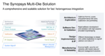
#61DAC was buzzing with discussion of chiplet-based, heterogeneous design. This new design approach opens new opportunities for applications such as AI, autonomous driving and even quantum computing. A critical enabler for all this to work is reliable, cost-effective advanced packaging, and that is the topic of this post.… Read More
#61DAC is evolving. The big get bigger and ultimately focus on other venues for customer outreach and branding. This is a normal evolution in any industry. For EDA, it was noticed by many that Cadence and Synopsys have downsized their booths at DAC. Everyone knows CDNLive and SNUG are very successful events for these companies and… Read More
#61DAC was buzzing this year with talk of AI and multi-die, heterogeneous design. The promise of making 2.5/3D design and a chiplet ecosystem mainstream reality was the focus of a lot of the panels and presentations at the conference. AI is certainly a driver for this new design style, but the conversation was broader than just AI,… Read More
The theme of this year’s DAC was Chips to Systems which is a full circle type of thing since systems companies used to make their own chips. Old school computer companies were the biggest chip makers when I started in the semiconductor industry. IDMs like Motorola and Intel replaced them at the chip level. Shortly after I joined… Read More
Heterogeneous multi-die integration is gaining more momentum all the time. The limited roadmap offered by Moore’s Law monolithic, single-die integration has opened the door to a new era of more-than-Moore heterogeneous integration. The prospects offered by this new design paradigm are exciting and the entire ecosystem is… Read More
This year’s live semiconductor ecosystem conferences have been well attend and I expect the same for #61DAC next week. I will be at the conference from Sunday afternoon to Wednesday evening, if you would like to meet let me know. Networking is an important part of the semiconductor ecosystem so let’s make it happen.… Read More
Introduction of 2.5D and 3D multi-die based products are helping extend the boundaries of Moore’s Law, overcoming limitations in speed and capacity for high-end computational tasks. In spite of its critical function within the 3DIC paradigm, the interposer die’s role and related challenges are often neither fully comprehended… Read More
The TSMC Technology Symposium provides a worldwide stage for TSMC to showcase its advanced technology impact and the extensive ecosystem that is part of the company’s vast reach. These events occur around the world and the schedule is winding down. TSMC covers many topics at its Technology Symposium, including industry-leading… Read More


Chemical Origins of Environmental Modifications to MOR Lithographic Chemistry