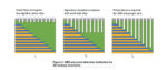
As process technologies have advanced, the difficulties in performing etch operations have increased. New structures and chemistries have created challenges in monitoring these complex operations. For instance, 3D-NAND structures call for high aspect ratio (HAR) trench etching. Likewise, in addition to involving Al, … Read More
Molecular Sensing for Semiconductor Etch Applications