Physics-Aware Intelligence: The Missing Layer Between Digital Twins and Governed Semiconductor Realization
The next stage of semiconductor scaling will not be driven only by smaller transistors, larger packages, more HBM, faster interconnects, or stronger cooling systems.It will also be driven by a new form of intelligence inside the engineering flow:
Physics-Aware Intelligence.
This does not mean generic AI optimization. It does not mean that AI independently approves semiconductor decisions. It does not mean replacing engineering judgment.
Physics-Aware Intelligence means using physical models, simulation outputs, EDA awareness engines, material behavior, workload projections, manufacturing history, test evidence, and runtime signals to identify physical risk before the system reaches failure, and often before full admissible evidence exists.
This is important because AI-era semiconductor systems are no longer isolated silicon products.
They are coupled physical systems.
A hotspot is not only a thermal issue. It can become a mechanical stress issue, a leakage issue, an aging issue, a package warpage issue, a power-delivery issue, a timing issue, and eventually a system-performance issue.
A firmware throttling action is not only a software policy. It can reshape workload placement, latency, current transients, link behavior, PDN response, thermal gradients, and reliability exposure across a cluster.
A new thermal material is not only a material choice. It can change heat flow, stress transfer, interface resistance, manufacturability, long-term aging, and field reliability.
This is why the industry is moving toward many forms of “aware” engineering:
power-aware design,
thermal-aware modeling,
stress-aware packaging,
manufacturing-aware optimization,
reliability-aware analysis,
EM-aware simulation,
material-aware integration,
and physics-informed AI.
This direction is correct.
But awareness is not the same as authority.
A power-aware tool may identify a voltage droop risk.
A thermal-aware model may identify a hotspot.
A stress-aware package model may identify a crack-risk region.
A material model may suggest better heat spreading.
A Physics AI model may predict thermal, mechanical, or electrical behavior before a prototype exists.
All of these are valuable.
But none of them should automatically close a design gate, approve a package architecture, relax a manufacturing guardband, change a firmware envelope, or qualify a field policy.
That is where the Governed System Digital Twin becomes important.
A traditional digital twin models a system.
A Governed System Digital Twin connects many domain twins, awareness engines, Physics AI outputs, material models, manufacturing evidence, test evidence, runtime telemetry, and field learning into one evidence path.
It is the digital convergence layer between physics prediction and governed decision authority.
Inside this structure, Physics-Aware Intelligence becomes an upstream intelligence layer.
It detects risk early.
It may say:
this package region may develop warpage,
this HBM stack may create thermal coupling risk,
this CPO module may experience optical alignment drift,
this CPAM power corridor may face anti-resonance under workload migration,
this System EM Corridor may lose margin under combined voltage noise and thermal drift,
this material stack may improve heat flow but create stress or reliability tradeoffs.
But the output is still a hypothesis.
It is not final evidence.
The Governed System Digital Twin must then convert that hypothesis into an evidence path.
That means asking:
What evidence is missing?
What test condition must be created?
Which boundary condition matters?
Which measurement confirms or falsifies the risk?
Is the evidence synchronized to the right realization state?
Does the causal chain make physical sense?
What uncertainty remains?
Is the evidence mature enough to support action?
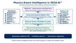
This is where SEGA-AI™ fits.
SEGA-AI™ is not just a dashboard.
It is not passive observability.
It is not generic AI automation.
SEGA-AI™ is the lifecycle governance architecture that determines whether evidence is mature, trusted, causally aligned, uncertainty-bounded, and safe enough to support a real semiconductor decision.
The top-down view is:
SEGA-AI™ defines the governance architecture.
The Governed System Digital Twin organizes model-to-evidence convergence.
Physics-Aware Intelligence detects risk and generates hypotheses.
Domain twins and awareness engines model physical behavior.
Manufacturing, prototype, test, runtime, and fleet systems generate evidence.
CEMH matures the evidence.
TCG verifies trust, provenance, synchronization, and causality.
Bounded Gate Authority determines whether the decision can close.
The bottom-up view is equally important:
Materials, devices, packages, boards, firmware, workloads, sensors, ATE, validation benches, and field systems produce signals.
Those signals become Evidence Objects.
Evidence Objects enter the Governed System Digital Twin.
The twin connects them to risk hypotheses, domain models, and causality paths.
SEGA-AI™ determines whether they are admissible enough to support authority.
This creates a complete top-to-bottom and bottom-to-top architecture.
It also changes how we think about new technologies.
Take substrate-level thermal transport, such as phononic or phonon-engineered approaches. The key idea is not only “better cooling.” It is that heat transport inside the silicon or substrate may become an engineered design parameter.
Take patternable high-thermal-conductivity materials. The key idea is not only higher thermal conductivity. It is selective heat routing: guiding heat away from hotspots, protecting sensitive regions, and creating intentional thermal paths through the package.
Take silicone, LSR, or other functional interface materials. The key issue is not only material selection. These materials can affect thermal flow, stress relief, vibration, sealing, EMC behavior, adhesion, aging, manufacturability, and reliability.
In all of these cases, Physics-Aware Intelligence can help predict where the technology may help and where it may create secondary risk.
But SEGA-AI™ must govern whether the claim becomes trusted evidence.
That distinction matters.
Cooling removes heat.
Thermal materials can route heat.
Substrate engineering may control how heat moves.
Physics-Aware Intelligence predicts the consequence.
Governed System Digital Twin organizes the evidence path.
SEGA-AI™ determines whether the evidence is mature enough to act.
This is also where active evidence generation becomes important.
If the system detects a critical risk but lacks evidence, it should not wait passively for a future failure. It should generate an evidence request.
For example:
If a CPAM power corridor may face anti-resonance under a fast dI/dt burst, the system should request evidence for that condition.
If an HBM stack may face thermal coupling under a specific memory-bank activity pattern, the system should request evidence for that workload.
If a package material may reduce hotspots but increase stress, the system should request thermal and mechanical evidence together.
If a CPO assembly may drift under thermal cycling, the system should request optical, thermal, and mechanical validation evidence under the same convergence epoch.
This does not mean uncontrolled autonomous testing.
It means bounded evidence creation.
The test must remain inside a Test Authority Envelope: safe operating limits, equipment constraints, firmware permissions, workload limits, human review thresholds, and escalation rules.
The principle is simple:
Do not guess.
Do not overtrust the model.
Do not wait for failure.
Generate the evidence required to decide.
This is the real value of Physics-Aware Intelligence inside SEGA-AI™.
It lets semiconductor systems become earlier, smarter, and more physically aware without becoming uncontrolled.
It allows prediction without premature authority.
It allows awareness without false confidence.
It allows active evidence generation without unsafe automation.
The final architecture is:
Awareness detects risk.
Physics-Aware Intelligence generates hypotheses.
The Governed System Digital Twin organizes the evidence path.
Manufacturing, test, runtime, and fleet systems generate evidence.
CEMH matures the evidence.
TCG verifies trust and causality.
Uncertainty bounds the decision.
Fleet Learning refines assumptions.
Bounded Gate Authority approves.
That is the bridge between digital twins and governed semiconductor realization.
The future will not be defined only by more models.
It will be defined by whether those models can converge with physics, materials, manufacturing, runtime behavior, and field evidence into trusted decision authority.
That is the role of Physics-Aware Intelligence inside the Governed System Digital Twin.
And that is why SEGA-AI™ is needed from top to bottom — and from bottom back to the top.