Samsung’s system chip, foundry business under close scrutiny for overhaul
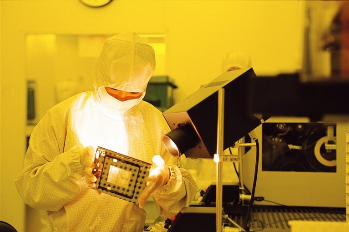
A researcher in a Samsung Electronics chip cleanroom
Samsung Electronics Co., the world’s largest memory chipmaker, has put its system chip and foundry businesses under tight scrutiny for a possible business overhaul, including an executive reshuffle and employee relocation, as it faces an uphill battle against rivals such as Taiwan’s TSMC.
The move underscores the urgency of bolstering competitiveness in a sector that has been the key focus of Chairman Lee Jae-yong’s long-term strategy but has struggled to gain ground against industry leaders, analysts said.
The South Korean tech giant’s Management Diagnosis Office in January began a thorough business review of its System LSI division, which specializes in chip design, people familiar with the matter said on Thursday.
Once a careful review of the division is over, the office plans to look into the firm’s foundry, or contract chipmaking, business, sources said.
(Graphics by Dongbeom Yun)
The business review marks Samsung’s first major internal audit since the company launched the office last November as part of its groupwide efforts to revive its struggling businesses.
Sources said the review signals a critical evaluation of Samsung’s strategy in non-memory semiconductors – an area the chairman, known as Jay Y. Lee in the international community, designated as a future growth engine back in 2019 under Samsung’s “System Semiconductor Vision 2030” initiative.
PERFORMANCE CONCERNS
While Samsung has made substantial investments in its system semiconductor business over the past few years, results have been mixed.
Its Exynos 2500 mobile processor failed to secure a spot inside the flagship Galaxy S25 smartphone, launched in January.
A Samsung employee examines a chip wafer
Samsung’s image sensors, the global market share of which is less than 20%, continue to lag behind Japan’s Sony.
The Korean chipmaker’s foundry business has struggled for years to compete with Taiwan Semiconductor Manufacturing Co. (TSMC), which maintains a dominant position in high-end semiconductor manufacturing.
As of the fourth quarter of 2024, Samsung, the world’s No. 2 foundry player, had 8.2% market share, compared with TSMC’s 67.1%.
The lack of progress has prompted Samsung to take a deeper look at its operations.
The management audit office, led by former Samsung SDI Co. CEO Choi Yoon-ho, has been tasked with evaluating the challenges facing Samsung Electronics’ key businesses and identifying strategies for improved competitiveness.
The office’s involvement is viewed by industry watchers as a step toward restoring a central corporate control structure akin to the former Samsung Future Strategy Office, which was dismantled in 2017.
TSMC is the world's largest foundry player
HEADWINDS
A key challenge for the System LSI division has been its inability to expand its customer base beyond the company’s own divisions – a situation highlighted by the Exynos 2500 mobile application processor’s exclusion from the Galaxy S25.
Similarly, while Samsung has made inroads in automotive semiconductors by supplying automotive Exynos chip to
Hyundai Motor Co. for the automaker’s infotainment system, it lost a key bid to Qualcomm for Hyundai’s self-driving chip supply contract.
In image sensors, Chinese smartphone makers, including Oppo, Vivo and Xiaomi, have increasingly turned to domestic suppliers, limiting Samsung’s market expansion opportunities.
Samsung has also faced difficulties in developing custom AI semiconductors – a critical area of future growth.
Its joint AI accelerator project with Naver Corp., known as Mach-1, has nearly stalled, and a second initiative, Mach-2, targeting Microsoft and other US Big Tech firms, has yet to yield results.
These setbacks have raised concerns about Samsung’s ability to compete with specialized players such as Broadcom and Marvell in the application-specific chip market.
Samsung's flag seen outside its headquarters in Seoul
FOUNDRY BUSINESS
Samsung’s foundry division, also set to undergo a management review, has been struggling with low production yields in advanced manufacturing nodes.
The company was the first to adopt gate-all-around (GAA) transistor technology in its 3-nanometer process, but low product yields have prevented it from securing major customers.
Samsung’s Shell-First Strategy, a custom-tailored new operation strategy, is also struggling as the chipmaker has failed to secure enough foundry clients.
Samsung’s foundry business posted more than 2 trillion won ($1.4 billion) in operating losses in the fourth quarter of 2024.
The company’s $37 billion investment in a US fab in Taylor, Texas, has also faced delays, with production now pushed back by two years to 2026.
With TSMC recently announcing a $100 billion expansion plan in the US, concerns are mounting over whether Samsung can attract enough high-profile customers to justify its investment, analysts said.
Samsung faces an uphill battle in advanced AI chip competiton
ORGANIZATIONAL RESTRUCTURING, PERSONNEL RESHUFFLE
Samsung’s business review is expected to lead to significant changes within the System LSI division.
One possibility under consideration is handing over the Exynos system-on-chip (SoC) business from the System LSI division to the Mobile eXperience (MX) division, aligning it more closely with Samsung’s smartphone strategy, sources said.
In the image sensor segment, the company may pivot from competition for high-resolution products and focus instead on products tailored for autonomous vehicles and robotics, they said.
Samsung’s System LSI recently set up a team tasked with securing a deal to supply image sensors to Apple Inc. as early as next year.
Samsung Electronics' chip cleanroom
For the foundry business, Samsung plans to assess the feasibility of its paused investments in its Korean plant in Pyeongtaek as well as Taylor.
The chipmaker also aims to work out a strategy to improve product yields in advanced nodes and secure AI chip manufacturing contracts, sources said.
To achieve these goals, Samsung may reshuffle executives and researchers at its System LSI division, including foundry workers, they said.
Samsung Electronics Co., the world’s largest memory chipmaker, has put its system chip and foundry businesses under tight scrutiny for a possible busines

www.kedglobal.com

 www.trendforce.com

")