Array
(
    [content] =>
    [params] => Array
        (
            [0] => /forum/threads/micron-announces-232-layer-nand.16447/
        )

    [addOns] => Array
        (
            [DL6/MLTP] => 13
            [Hampel/TimeZoneDebug] => 1000070
            [SV/ChangePostDate] => 2010200
            [SemiWiki/EmailDomainReplace] => 1000010
            [SemiWiki/Newsletter] => 1000010
            [SemiWiki/WPMenu] => 1000010
            [SemiWiki/XPressExtend] => 1000010
            [ThemeHouse/XLink] => 1000970
            [ThemeHouse/XPress] => 1010570
            [XF] => 2031070
            [XFI] => 1060170
        )

    [wordpress] => /var/www/html
)
You are currently viewing SemiWiki as a guest which gives you limited access to the site. To view blog comments and experience other SemiWiki features you must be a registered member. Registration is fast, simple, and absolutely free so please,
join our community today !
JavaScript is disabled. For a better experience, please enable JavaScript in your browser before proceeding.
You are using an out of date browser. It may not display this or other websites correctly.
You should upgrade or use an
alternative browser .
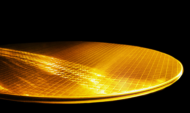
Micron announces 232 layer NAND
www.anandtech.com
For a double-stacked structure, this NAND process etches more than 100 layers at a time. It used to be only Samsung could do this.
Moreover, two controllers (one internally designed, one externally designed) are supporting this NAND. Likely using FinFET nodes.