You are currently viewing SemiWiki as a guest which gives you limited access to the site. To view blog comments and experience other SemiWiki features you must be a registered member. Registration is fast, simple, and absolutely free so please, join our community today!
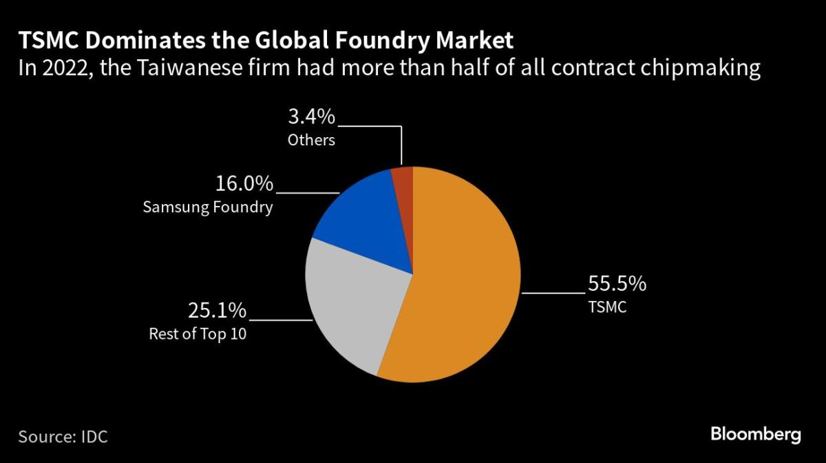
Are Samsung and Rapidus really using IBM's 3nm/2nm technology to the similar degree?
"“Rapidus and Samsung are on the same platform as they both use IBM technology, and it’s very possible the two can strike a win-win partnership as their business models are quite different,” Omdia analyst Akira Minamikawa said."
(Bloomberg) -- International Business Machines Corp. is prioritizing helping Japan’s chipmaking startup Rapidus Corp., with a senior executive describing the budding foundry business as vital to securing long-term global supply.Most Read from BloombergTesla and BYD Post Record Sales on Surge in...
“We know from our own experience that providing the newest generation of chips is not something that one company can handle alone,” he said. “Both TSMC and Samsung will welcome Rapidus joining the club of cutting-edge chip manufacturers because, as things stand now, they are making customers wait. Rapidus taking some orders from them wouldn’t be a problem.”
I can hear TSMC and Samsung now... "We don't want an order backlog, we'd much rather have Rapidus take some of that business to better satisfy our customers!"
I can hear TSMC and Samsung now... "We don't want an order backlog, we'd much rather have Rapidus take some of that business to better satisfy our customers!"
No. Samsung and IBM seem to collaborate on CR, but they don't seem to licence. In my opinion, the nodes Samsung makes differ too much from the IBM process technology to say it is an IBM node. For example from memory Samsung's 14LPP had different pitches from the common platform alliance 14nm paper. Even back when they were indisputably more in tune with the common platform alliance in the pre gate first catastrophe, they never really embraced SOI like the other non UMC members did. Finally IBM/GF's 7nm paper which made an extensive use of cobalt for the lower vias (or maybe it was a Co linner I can't properly recall). Samsung on the other hand to my knowledge only used Cu vias/metal lines. They did however make extensive use of EUV like the IBM/GF CR 7nm whitepaper did. As for 2"nm", Samsung said they were going to 4 nanosheets and adding the option of BSPD. IBM's 2"nm" was only three sheets, first gen GAA, did not have support for BSPD, and did RMG differently. Samsung also claimed a 5% shrink for SF2 over SF3 (aka 3GAP), which should lead to lower densities than IBM's 2"nm"
On the other hand Rapidus said they were "licencing IBM's 2nm" and trying to "bring it to production". To me Samsung's approach sounds very different than what Rapidus is doing. Although who knows; for all we know Rapidus has to change so much to get it manufacturable that it barely resembles IBM's node anymore.
I can hear TSMC and Samsung now... "We don't want an order backlog, we'd much rather have Rapidus take some of that business to better satisfy our customers!"
Yeah this whole article had me scratching my head big time. Very nonsensical. I don’t know of anyone who is really taking Rapidus seriously at all. IBM is not a fabrication powerhouse by a long shot. They do research and not particularly economical processes judging by how its global foundries partnership turned out.
"TSMC Chairman Mark Liu has said he doesn’t see Rapidus as a competitor, as the Japanese chipmaker will focus on fostering engineering talent."
I don't know about the foundry business but early in my career IBM and Japan were ASIC giants.
Even if the IBM/IMEC 2nm process does yield in a timely manner, which is a VERY big if, I really do not see them being competitive against TSMC in the foundry business. Maybe doing ASICs for Japan customers or narrow markets for captive customers (investors). It should be fun to watch though, IBM always is: IBM, the press release leader for process technologies!
 finance.yahoo.com
