





In a major bid to bypass crippling U.S. technology sanctions, China’s Huawei Technologies has unveiled an ambitious semiconductor roadmap, projecting the design of high-end chips with a transistor density equivalent to a 1.4-nanometer (1.4-nm) process node by 2031.
The announcement was made on Monday, May 25, 2026, by He Tingbo—President of Huawei’s HiSilicon semiconductor division and chair of the company’s Scientist Committee—during a keynote speech at the 2026 IEEE International Symposium on Circuits and Systems (ISCAS) in Shanghai.
To overcome this, Huawei introduced a new architectural framework called the Tau ($\tau$) Scaling Law (referred to by some industry peers as He’s Law).
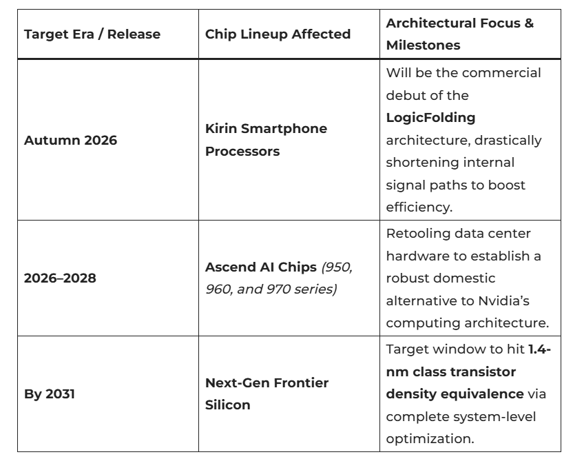
The upcoming deployment schedule aims to directly challenge Western silicon pacesetters:
On one hand, tech firms like TSMC are already targeting true, native 1.4-nm physical mass production by 2028. Huawei’s 2031 timeline for density equivalence means China will technically remain a few years behind the absolute global manufacturing frontier. Furthermore, Huawei has not yet published independent, third-party performance or toxicological yield data to validate its laboratory benchmarks.
On the other hand, industry experts from firms like Omdia point out that system-level scaling—relying on advanced packaging, 3D chiplet stacking, and signal path compression—is a highly credible way to squeeze bleeding-edge performance out of older, legally available manufacturing equipment. By formalizing the Tau Scaling Law, Huawei is building a vital blueprint to insulate China’s domestic AI, smartphone, and supercomputing infrastructure from future Western trade embargoes.
The announcement was made on Monday, May 25, 2026, by He Tingbo—President of Huawei’s HiSilicon semiconductor division and chair of the company’s Scientist Committee—during a keynote speech at the 2026 IEEE International Symposium on Circuits and Systems (ISCAS) in Shanghai.
1. The Strategy: Sidestepping Traditional Moore’s Law
Because Washington has strictly blocked China’s access to advanced Extreme Ultraviolet (EUV) lithography equipment from ASML, Chinese foundries cannot easily manufacture chips using traditional geometric shrinking.To overcome this, Huawei introduced a new architectural framework called the Tau ($\tau$) Scaling Law (referred to by some industry peers as He’s Law).
- Time Over Geometry: Traditional chip scaling relies on making transistors physically smaller (node scaling). The Tau Scaling Law flips the script by focusing on system-level efficiency scaling—specifically cutting down the time (latency) it takes for data and electronic signals to propagate through devices, circuits, and systems.
- The LogicFolding Solution: Alongside the scaling law, Huawei unveiled its LogicFolding architecture. This design dramatically shortens the physical wiring inside a chip, reducing resistive and capacitive loads. By stacking silicon and optimizing internal interconnects, Huawei claims it can mimic the performance and transistor density of a 1.4-nm node without requiring the tight sub-atomic physical engraving of Western foundries.
2. Slicing Open the Roadmap: 2026 to 2031
Huawei stressed that this isn’t just a theoretical research paper. The company claims it has quietly designed and mass-produced 381 distinct chips over the past six years utilizing early variations of this system-level architecture.The upcoming deployment schedule aims to directly challenge Western silicon pacesetters:
3. Industry Realism vs. Geopolitical Insulations
Independent semiconductor analysts view Huawei’s 1.4-nm equivalent target with a mix of fascination and caution.On one hand, tech firms like TSMC are already targeting true, native 1.4-nm physical mass production by 2028. Huawei’s 2031 timeline for density equivalence means China will technically remain a few years behind the absolute global manufacturing frontier. Furthermore, Huawei has not yet published independent, third-party performance or toxicological yield data to validate its laboratory benchmarks.
On the other hand, industry experts from firms like Omdia point out that system-level scaling—relying on advanced packaging, 3D chiplet stacking, and signal path compression—is a highly credible way to squeeze bleeding-edge performance out of older, legally available manufacturing equipment. By formalizing the Tau Scaling Law, Huawei is building a vital blueprint to insulate China’s domestic AI, smartphone, and supercomputing infrastructure from future Western trade embargoes.

