News from the "Coal Face"
SINGAPORE – EUV Tech, a major US-based manufacturer of extreme ultraviolet metrology equipment essential for cutting-edge semiconductor manufacturing, has opened its first global office here on Jan 28.
Located at Mapletree Hi-Tech Park @ Kallang Way, the office will serve as a regional hub, strengthening the company’s global footprint and boosting its ability to serve customers here as well as across key Asian markets such as South Korea, Japan and Taiwan.
Extreme ultraviolet light is used in advanced semiconductor manufacturing to print tiny circuit patterns onto wafers, with photomasks acting like stencils to guide the process. EUV Tech’s metrology tools are used to inspect the quality of photomasks.
Speaking at the opening ceremony, chief executive Patrick Naulleau said it was important to “be where the customers are”.
“It allows us to ensure productivity, make sure that we keep at the leading edge of this technology.
“If you’re not at the leading edge of this technology, you’re nowhere,” he said.
Asia is home to some of the world’s largest advanced semiconductor players, such as Taiwan Semiconductor Manufacturing Company and South Korea’s Samsung and SK Hynix.
The firm serves clients such as Japan’s HOYA Electronics, which develops optical and extreme ultraviolet photomask blanks used in manufacturing the latest-generation chips critical for various applications such as artificial intelligence and high-performance computing.
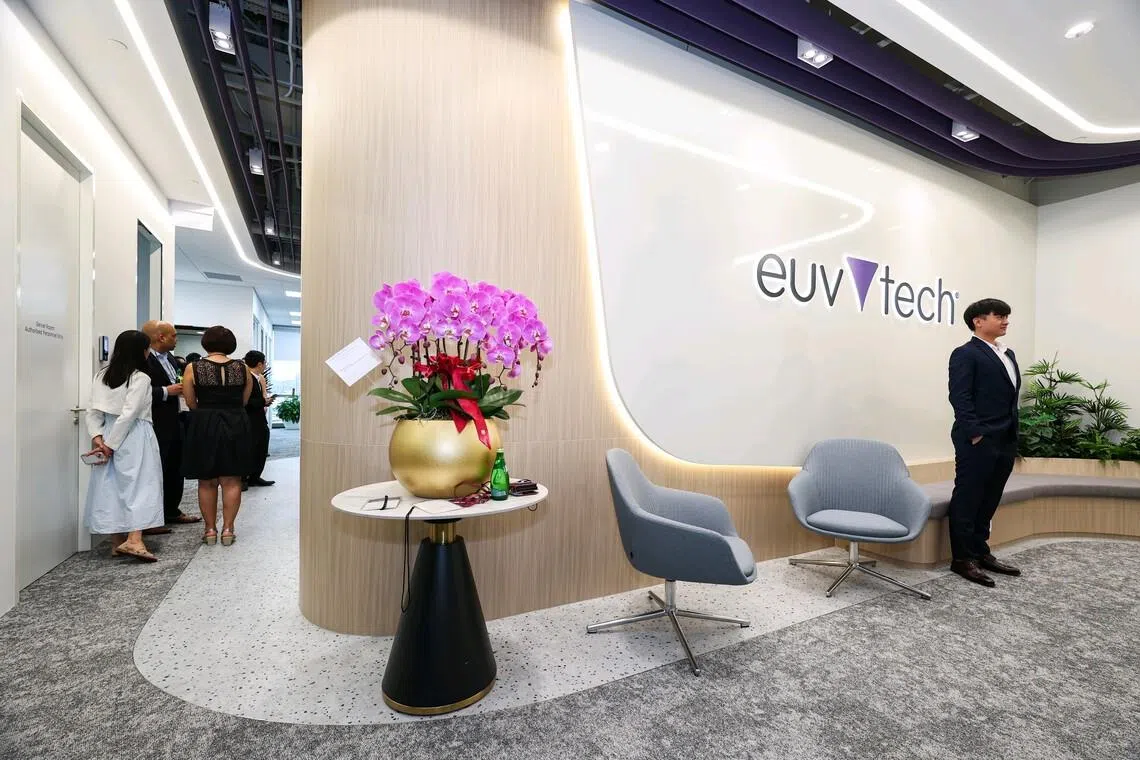
EUV Tech opened its first global office in Singapore on Jan 28.
ST PHOTO: BRIAN TEO
“As demand for leading-edge computer chips goes up, more photomasks are needed, so the demand for EUV Tech’s equipment also goes up. Our growth is basically proportional to the leading-edge semiconductor manufacturing industry’s growth,” Dr Naulleau told The Straits Times.
The firm has no immediate plans to relocate research and development here, but Dr Naulleau said he has been engaging local universities to explore potential opportunities.
EUV Tech plans to hire 10 or more employees in Singapore over the next three years in roles such as field service engineering and software engineering. It will also develop local talent by offering internship opportunities for students from institutes of higher learning.
Economic Development Board (EDB) vice-president of global enterprises Soo Haw Yun said the new set-up is a welcome addition to Singapore’s semiconductor ecosystem.
“(EUV Tech’s new office will provide) better support and service to its customers in the region and will create new technical and customer-facing roles, including in field engineering, software engineering and customer success,” said Mr Soo.
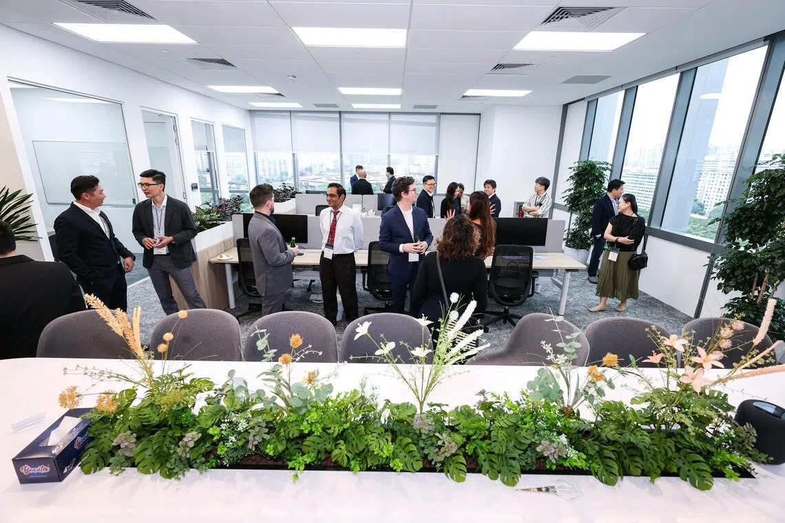
EUV Tech’s new office will serve as a regional hub, strengthening the company’s global footprint and boosting its ability to serve customers here as well as across key Asian markets such as South Korea, Japan and Taiwan.
ST PHOTO: BRIAN TEO
Singapore accounts for one in 10 chips in the global semiconductor supply chain, and one-fifth of global semiconductor equipment production.
An EDB spokesman said: “In the past two years, Singapore has been successful in attracting over $18 billion of research and development and manufacturing investments into our semiconductor ecosystem. These investments will generate good businesses and job opportunities for Singapore.”
https://www.straitstimes.com/busine...lobal-office-in-spore-to-serve-asia-customers
SINGAPORE – EUV Tech, a major US-based manufacturer of extreme ultraviolet metrology equipment essential for cutting-edge semiconductor manufacturing, has opened its first global office here on Jan 28.
Located at Mapletree Hi-Tech Park @ Kallang Way, the office will serve as a regional hub, strengthening the company’s global footprint and boosting its ability to serve customers here as well as across key Asian markets such as South Korea, Japan and Taiwan.
Extreme ultraviolet light is used in advanced semiconductor manufacturing to print tiny circuit patterns onto wafers, with photomasks acting like stencils to guide the process. EUV Tech’s metrology tools are used to inspect the quality of photomasks.
Speaking at the opening ceremony, chief executive Patrick Naulleau said it was important to “be where the customers are”.
“It allows us to ensure productivity, make sure that we keep at the leading edge of this technology.
“If you’re not at the leading edge of this technology, you’re nowhere,” he said.
Asia is home to some of the world’s largest advanced semiconductor players, such as Taiwan Semiconductor Manufacturing Company and South Korea’s Samsung and SK Hynix.
The firm serves clients such as Japan’s HOYA Electronics, which develops optical and extreme ultraviolet photomask blanks used in manufacturing the latest-generation chips critical for various applications such as artificial intelligence and high-performance computing.
EUV Tech opened its first global office in Singapore on Jan 28.
ST PHOTO: BRIAN TEO
“As demand for leading-edge computer chips goes up, more photomasks are needed, so the demand for EUV Tech’s equipment also goes up. Our growth is basically proportional to the leading-edge semiconductor manufacturing industry’s growth,” Dr Naulleau told The Straits Times.
The firm has no immediate plans to relocate research and development here, but Dr Naulleau said he has been engaging local universities to explore potential opportunities.
EUV Tech plans to hire 10 or more employees in Singapore over the next three years in roles such as field service engineering and software engineering. It will also develop local talent by offering internship opportunities for students from institutes of higher learning.
Economic Development Board (EDB) vice-president of global enterprises Soo Haw Yun said the new set-up is a welcome addition to Singapore’s semiconductor ecosystem.
“(EUV Tech’s new office will provide) better support and service to its customers in the region and will create new technical and customer-facing roles, including in field engineering, software engineering and customer success,” said Mr Soo.
EUV Tech’s new office will serve as a regional hub, strengthening the company’s global footprint and boosting its ability to serve customers here as well as across key Asian markets such as South Korea, Japan and Taiwan.
ST PHOTO: BRIAN TEO
Singapore accounts for one in 10 chips in the global semiconductor supply chain, and one-fifth of global semiconductor equipment production.
An EDB spokesman said: “In the past two years, Singapore has been successful in attracting over $18 billion of research and development and manufacturing investments into our semiconductor ecosystem. These investments will generate good businesses and job opportunities for Singapore.”
https://www.straitstimes.com/busine...lobal-office-in-spore-to-serve-asia-customers