Array
(
    [content] =>
    [params] => Array
        (
            [0] => /forum/threads/cxmt-claims-to-make-18-5nm-not-17nm-dram.19541/
        )

    [addOns] => Array
        (
            [DL6/MLTP] => 13
            [Hampel/TimeZoneDebug] => 1000070
            [SV/ChangePostDate] => 2010200
            [SemiWiki/EmailDomainReplace] => 1000010
            [SemiWiki/Newsletter] => 1000010
            [SemiWiki/WPMenu] => 1000010
            [SemiWiki/XPressExtend] => 1000010
            [ThemeHouse/XLink] => 1000970
            [ThemeHouse/XPress] => 1010570
            [XF] => 2031070
            [XFI] => 1060170
        )

    [wordpress] => /var/www/html
)
You are currently viewing SemiWiki as a guest which gives you limited access to the site. To view blog comments and experience other SemiWiki features you must be a registered member. Registration is fast, simple, and absolutely free so please,
join our community today !
JavaScript is disabled. For a better experience, please enable JavaScript in your browser before proceeding.
You are using an out of date browser. It may not display this or other websites correctly.
You should upgrade or use an
alternative browser .
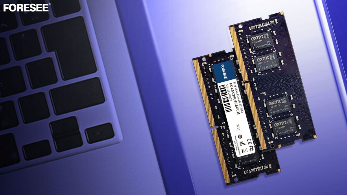
CXMT claims to make 18.5nm not 17nm DRAM
As CXMT preps to expand production capacity, it has to comply with U.S. requirements.
www.tomshardware.com
CXMT, China's champion DRAM company, is portraying a previously touted 17nm technology as 18.5nm, thereby circumventing sanctions.
Is there a definition of what DRAM node names mean?
Is there a definition of what DRAM node names mean?
It is supposed to be half-pitch of active area. That makes this attempted re-definition quite humorous.
They shouldn't sandbag if they're going to get caught.