CPO and optical I/O are often described as “light replacing copper.”
I think that framing is incomplete.
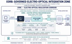
Before data becomes optical, the electrical launch still has to close. After conversion, the optical path still has to be attached, powered, aligned, cooled, coupled to fiber, tested, and qualified.
That is why I frame this as an Electro-Optical Realization Block, or EORB, inside a broader Electro-Optical Realization Corridor.
The modulator or optical engine may be the device breakthrough. But the product is the full realization path:
electrical launch
optical conversion
driver integration
package/substrate interface
alignment stability
thermal drift control
fiber attach
SI/PI behavior
test coverage
yield learning
lifecycle reliability
This is especially important for CPO, silicon photonics, and future AI/HPC optical interconnects.
The winning architecture will not be the one with the best optical device alone. It will be the one that proves the full electro-optical corridor can be manufactured, tested, cooled, aligned, and trusted at scale.
Light may solve distance.
Governed electro-optical realization determines whether it scales.
I think that framing is incomplete.
Before data becomes optical, the electrical launch still has to close. After conversion, the optical path still has to be attached, powered, aligned, cooled, coupled to fiber, tested, and qualified.
That is why I frame this as an Electro-Optical Realization Block, or EORB, inside a broader Electro-Optical Realization Corridor.
The modulator or optical engine may be the device breakthrough. But the product is the full realization path:
electrical launch
optical conversion
driver integration
package/substrate interface
alignment stability
thermal drift control
fiber attach
SI/PI behavior
test coverage
yield learning
lifecycle reliability
This is especially important for CPO, silicon photonics, and future AI/HPC optical interconnects.
The winning architecture will not be the one with the best optical device alone. It will be the one that proves the full electro-optical corridor can be manufactured, tested, cooled, aligned, and trusted at scale.
Light may solve distance.
Governed electro-optical realization determines whether it scales.