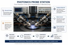
From Photonics Precision to Repeatable Evidence
Silicon photonics has already proven that extremely precise optical alignment is possible.In the lab, engineers can align fibers, probes, waveguides, grating couplers, edge couplers, modulators, and detectors with very high accuracy. They can measure insertion loss, coupling efficiency, optical power, bandwidth, modulation response, and device behavior under controlled conditions.
That level of precision is impressive.
But precision alone does not create scale.
The harder question is whether the same optical result can be repeated again and again across many devices, many wafers, many operators, many tools, and many production lots.
This is where photonics probing becomes important.
A photonics probe platform is not just a laboratory instrument. It is a transition point between R&D success and manufacturing confidence.
It brings together optical alignment, electrical probing, imaging, motion control, calibration, measurement automation, and repeatability. The device under test may be a photonic die, wafer, optical engine, modulator, detector, or integrated silicon photonics structure. The system must align light into and out of the device while also measuring electrical behavior.
That is not trivial.
In electronics, probing a pad is already a precision task. In photonics, the challenge is more sensitive because small shifts in position, height, angle, polarization, temperature, or coupling condition can change the measured result.
A good measurement once is useful.
A repeatable measurement thousands of times is evidence.
That is the important shift.
Photonics manufacturing does not only need better optical devices. It needs repeatable optical test, repeatable coupling, repeatable alignment, repeatable calibration, and repeatable measurement conditions.
This is why platforms such as photonics probe stations matter. They help move silicon photonics from expert-driven lab alignment toward controlled, repeatable, and automatable measurement.
In our realization language, this is a key evidence step.
The photonic device may be good.
The optical coupling may work.
The modulator may perform.
The detector may respond.
But the product is not trusted until the measurement can be repeated, the variation can be understood, and the evidence can support a manufacturing or release decision.
Precision creates the first result.
Repeatability creates confidence.
Confidence creates manufacturing evidence.
Manufacturing evidence enables scale.
For CPO, optical I/O, silicon photonics, and photonic integrated circuits, this is one of the hidden realization boundaries.
The industry does not only need to prove that light can be aligned once.
It needs to prove that light can be aligned, measured, calibrated, and trusted repeatedly across production.
That is where photonics probing becomes more than test.
It becomes part of the realization evidence path.