You are currently viewing SemiWiki as a guest which gives you limited access to the site. To view blog comments and experience other SemiWiki features you must be a registered member. Registration is fast, simple, and absolutely free so please,
join our community today!
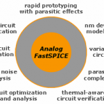
In working with TSMC and GlobalFoundries on AMS design reference flows I have experienced first hand the increasing verification challenges of nanometer analog, RF, and mixed-signal circuits. Tools in this area have to be both silicon accurate and blindingly fast! Berkeley Design Automation is one of the key vendors in this … Read More
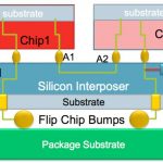
Going up! Power and performance issues, along with manufacturing yield issues, limit how much bigger chips can get in two dimensions. That, and the fact that you can’t manufacture two different processes on the same wafer, mean that we are going up into the third dimension.
The simplest way is what is called package-in-package… Read More
I went to the second Global Technology Conference yesterday. It started with a keynote by Ajit Manocha who is the CEO of about 2 months. I hadn’t realized until someone asked him during the press lunch that he is technically only the “acting” CEO. Actually, given his experience he might be the right person anyway,… Read More
The economic news lately has been bleak. U.S. GDP grew at an anemic 0.4% in 1Q 2011 and 1.0% in 2Q 2011 – leading to increased concerns about a double-dip recession. High government debt levels in the U.S. and several European nations have contributed to volatile stock markets. The news does not seem to be any better for the semiconductor… Read More
Verifying circuits on advanced process nodes has always been difficult, and it’s no easier with today’s nanometer CMOS processes. There’s a great paradox in nanometer circuit design and verification. Designers achieve their greatest differentiation when they implement analog, mixed-signal, RF and custom … Read More
Introduction
Mentor Graphics and GLOBALFOUNDRIES have been working together for several generations since the 65nm node on making IC designs yield higher. Michael Buehler-Garcia, director of Calibre Design SolutionsMarketing at Mentor Graphics spoke with me by phone today to explain how they are working with GLOBALFOUNDRIES… Read More
20nm SoC Designby Paul McLellan on 08-25-2011 at 12:48 amCategories: Uncategorized
There are a large number of challenges at 20nm that didn’t exist at 45nm or even 32nm.
The biggest issues are in the lithography area. Until now it has been possible to make a reticle using advanced reticle enhacement technology (RET) decoration and have it print. Amazing when you think that at 45nm we are making 45nm features… Read More
Silicon Oneby Paul McLellan on 08-23-2011 at 5:23 pmCategories: Uncategorized
I have talked quite a bit over the last few years about how the trend towards small consumer devices with very fast ramp times. For example, pretty much any time Apple introduces a new product line (iPod, iPhone, iPad…) it becomes the fastest growing market in history. This has major implications for semiconductor design … Read More
Last month I had the pleasure of meeting Mr Wonyoung Kim, a PhD candidate from Harvard University. Like many candidates, Wonyoung is shopping his thesis for capital in hopes of starting a semiconductor IP company. Here is a brief summary of the technology, please provide appropriate feedback and let’s see if we can get him… Read More