You are currently viewing SemiWiki as a guest which gives you limited access to the site. To view blog comments and experience other SemiWiki features you must be a registered member. Registration is fast, simple, and absolutely free so please,
join our community today!
Sign up for a free webinar on December 11 on Accelerating Yield and Failure Analysis with Diagnosis.
The one hour presentation will be delivered via webcast by Geir Eide, Mentor’s foremost expert in yield learning. He will cover scan diagnosis, a software-based technique, that effectively identifies defects in digital logic… Read More
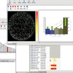
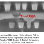
Finding and debugging failures on integrated circuits has become increasingly difficult. Two sessions at ISTFA (International Symposium for Testing and Failure Analysis) on Thursday address the current best practices and research directions of diagnosis.
The first was a tutorial this morning by Mentor Graphics luminary… Read More
Test is the Rodney Dangerfield of EDA, it doesn’t get any respect. All designs need to be tested but somehow synthesis, routing, analog layout and the rest are the sexy areas. In my spoof all purpose EDA keynote address I even dissed it:You are short on time so slip in a quick mention of manufacturing test. Who knows anything … Read More
Most of us live perfectly good lives without distinction, fame, or note. Others rack up the honors, filling their walls and resumes with recognition of their brilliance. Like Dr. Janusz Rajski.
Rajski is the director of engineering for the test products at Mentor Graphics, an IEEE Fellow, and the inventor of embedded deterministic… Read More
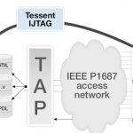
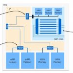
Benjamin Franklin, “I didn’t fail the test, I just found 100 ways to do it wrong.” I was reminded of this line during a joint Mentor-ARM seminar yesterday about testing ARM cores and memories. The complexity of testing modern SoC designs at advanced nodes, with multiple integrated ARM cores and other IP, opens up plenty of room for… Read More
If you are involved in testing memory or logic of ARM-based designs, you’ll want to attend this free seminar on July 17, 2012 in Santa Clara. Mentor Graphics and ARM have a long standing partnership, and have optimized the Mentor test products (a.k.a Tessent) for the ARM processors and memory IP.
The lunch seminar runs from 10:30-1:00… Read More
SEMICON West is coming up this July 10-12 at the Moscone Center in San Francisco. It covers a broad swath of the microelectronics supply chain, but I was particularly interested in the test sessions. Here are two that I recommend.
“The Value of Test for Semiconductor Yield Learning” on Tuesday, July 10, at 1:30p. The… Read More
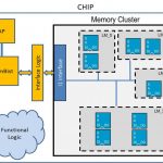
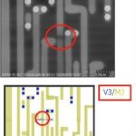
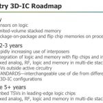
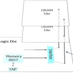
3D and 2.5D (silicon interposer) designs create new challenges for EDA. Not all of them are in the most obvious areas. Mentor has an interesting presentation on what is required for verification and testing of these types of designs. Obviously it is somewhat Mentor-centric but in laying out the challenges it is pretty much agnostic.… Read More
3D ICs complicate silicon testing, but solutions exist now to many of the key challenges. – by Stephen Pateras
The next phase of semiconductor designs will see the adoption of 3D IC packages, vertical stacks of multiple bare die connected directly though the silicon. Through-silicon vias (TSV) result in shorter and thinner… Read More