You are currently viewing SemiWiki as a guest which gives you limited access to the site. To view blog comments and experience other SemiWiki features you must be a registered member. Registration is fast, simple, and absolutely free so please,
join our community today!
We have posted several blogs related to Cadence IP strategy, or I should say new strategy. Each of these blogs was dealing with a particular product, like PCI Express gen-3 Controller IP, latest DDR4 Memory Controller or Wide I/O. This approach was equivalent to describe trees, one after one, and finally ignoring the forest! It’s… Read More
Yesterday Cadence had their annual front-end summit, the theme of which was physically aware design. I was especially interested in the first couple of presentations about physically aware synthesis. I joined Cadence in 1999 when they acquired Ambit Design Systems. One of the products that we had in development was called PKS… Read More
In an environment of SoCs with tough targets of multiple functionalities, smallest size, lowest power and fastest performance to achieve within a limited design cycle window in order to meet the rigid time-to-market requirements, any day spent without success becomes very frustrating for a designer. Especially during tape-out… Read More
Now a day, a SoC can be highly complex, having 100s of IPs performing various functionalities along with multi-core CPUs on it. Managing power, performance and area of the overall semiconductor design in the SoC becomes an extremely challenging task. Even if the IPs and various design blocks are highly optimized within themselves,… Read More
Save closure time and boost performance by incorporating knowledge of physically aware design early into your front-end design implementation flow
With the adoption of advanced process nodes, design closure is becoming increasingly difficult due to the lack of convergence between the front end and the back end of the register-transfer… Read More
Yesterday Cadence had an all-day Signoff Summit where they talked about the tools that they have for signoff in advanced nodes. Well, of course, those tools work just fine in non-advanced nodes too, but at 20nm and 16nm there are FinFETs, double patterning, timing impacts from dummy metal fill, a gazillion corners to be analyzed… Read More
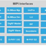
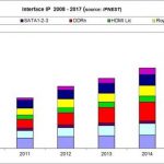
How to best forecast a specific protocol adoption? One option is to look at the various IP sales, it will give you a good idea of the number of SoC or IC offering this feature on the market in the next 12 months. Once again, if you wait for the IP sale to have reached a maximum, it will be too late, so you have to monitor the IP sales dynamic when… Read More
In EDA we have come to expect that only small start-up companies create new tools, however a team at Cadencehas developed a new IC power integrity tool called Voltus from scratch. To learn more I spoke last week with KT Moore, a Group Director at Cadence. I’ve known KT for over a decade, and first met him when he was at Magma marketing… Read More
Milandr is a company based in Moscow that makes high reliability semiconductor components for the aerospace, automotive and consumer markets, primarily in Russia. They work with multiple foundries, including X-FAB and TSMC in technologies from 1um down to 65nm. Corporate headquarter and main IC design house is located in Russian… Read More
I was the VP marketing at VaST Systems Technology and then at Virtutech. Both companies sold virtual platform technology which consisted of two parts:
- an extremely fast processor emulation technology that actually worked by doing a binary translation of the target binary code (e.g. an ARM) into the native instruction set of the
…
Read More