At CDNLive, Bob Mullen of TSMC gave a presentation on their new custom FinFET flow, doing design, and verifying designs. At 16nm there are all sorts of relatively new verification problems such as layout dependent effects (LDE) and voltage dependent design rules. We had some of this at 20nm but like most things in semiconductor,… Read More

Tag: cadence
Automating Analog Verification in Virtuoso
Digital designers have been automating the functional verification process for many years now, however when you talk to an analog designer about how they do verification you quickly realize that the typical process is quite ad-hoc and little automated. Necessity does create an opportunity so the software engineers at Methodics… Read More
ARM, Cadence and the Internet of Things

There is clearly a lot of hype about the Internet of Things (IoT) right now, but also it is clear that it will be a real market. In fact, it already is with various medical, fitness and home-appliance products already available. At CES in January, wearables was probably the biggest trend. That doesn’t always pan out (3D TV was… Read More
Cadence and ARM BFF

The biggest market for semiconductors is mobile and an ARM processor is the center of the axle around which it revolves. So everyone in the mobile ecosystem needs to work closely with ARM. At CDNLive earlier this week Cadence and ARM announced that they are deepening their partnership. Most of what they announced makes it a lot easier… Read More
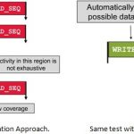
Effective Verification Coverage through UVM & MDV
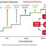
In the current semiconductor design landscape, the design size and complexity of SoCs has grown to large extent with stable tools and technologies that can take care of integrating several IPs together. With that mammoth growth in designs, verification flows are evolving continuously to tackle the verification challenges … Read More
Automating PCB Timing Closure, Saving Up to 67%
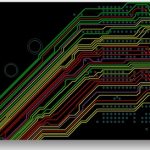
The benefits of using EDA software is that it can automate a manual process, like PCB timing closure, saving you both time and engineering effort. This point was demonstrated today as Cadenceadded new timing-closure automation to their Allegroproduct family, calling it Allegro TimingVision. On Tuesday I spoke with Hemant Shah… Read More
SoC Functional Verification Planning and Management Goes Big
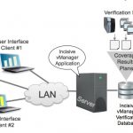
Big SoC designs typically break existing EDA tools and old methodologies, which then give rise to new EDA tools and methodologies out of necessity. Such is the case with the daunting task of verification planning and management where terabytes of data have simply swamped older EDA tools, making them unpleasant and ineffective… Read More
HDMI, DisplayPort, MHL IPs + Engineering Team = Good Move
This news is certainly not as amazing that the acquisition of MIPS by Imagination, or Arteris by Qualcomm… but it shows that Cadence is building a complete Interface IP port-folio, brick after brick. The result will be that a complete wall is being built on the Synopsys road to monopoly and complete success on Interface IP market.… Read More
Designing an SoC with 16nm FinFET
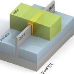
IC designers contemplating the transition to 16nm FinFET technology for their next SoC need to be informed about design flow and IP changes, so TSMC teamed up with Cadence Design Systems today to present a webinar on that topic. I attended the webinar and will summarize my findings.
Shown below is a 3D layout concept of an ideal FinFET… Read More
SoC Verification Closure Pushes New Paradigms
In the current decade of SoCs, semiconductor design size and complexity has grown by unprecedented scale in terms of gate density, number of IPs, memory blocks, analog and digital content and so on; and yet expected to increase further by many folds. Given that level of design, it’s imperative that SoC verification challenge has… Read More