
Samsung Foundry recently held their 4th annual technology forum in Santa Clara. This article reviews the highlights of the presentations. There were two prevalent themes throughout – focused execution on the current process roadmap, and the introduction of the 3nm process node features and schedule.
Before getting into the technical details, here is a brief review of the “new” Samsung Foundry. A timeline of the foundry services is appended below.
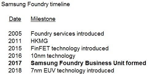
The 2017 milestone above is significant – the Samsung Foundry organization was created as a distinct business unit. Yongjoo Jeon, from the Samsung Foundry marketing team, explained, “Samsung Foundry operates independently from the company’s product divisions. We leverage the research progress of the R&D arm of Samsung Semiconductor – nevertheless, all customers are equal.”
Dr. E.S. Jung, President of Samsung Foundry, added, “We are focused on delivering exceptional foundry services – from our semiconductor and packaging technology roadmap, to our operational execution, to our strengthened IP capability and design services support. We are announcing design enablement on the cloud, as a result of our partnership with AWS and Azure, in collaboration with Cadence and Synopsys. We are proud of our 100% on-time delivery the past two years. There is a commitment to invest $100B in fabrication capabilities over the next 10 years. We are dedicated to becoming the most trusted foundry.”
Execution
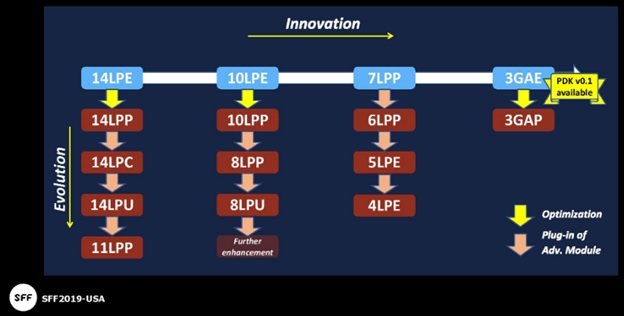
Here is a brief summary of the semiconductor process roadmap status. The axes on the figure below are the major process node updates (“Innovation”) and the incremental node enhancements (“Evolution”).
The typical nomenclature for a process node uses both an “Early” (E) and a “Performance” (P) designation.
14/11
- 2M+ wafer shipped, cumulative since 1Q’2015
- ”Initial customers were in mobile markets, now additional HPC and automotive applications are using these nodes.”
10/8
- 800K+ wafer shipped, cumulative since 4Q’2016
- HPC and mobile market applications initially, now additional consumer products
- “This will be a long-life node for very cost-sensitive products, until the cost cross-over occurs for 7nm.”
- 8LPP: 44nm Mx pitch
- 8LPU: ULVT, 1 fin standard cell template with both single- and double-diffusion break (8LPU introduced an ULVT device for HPC applications, compared to 8LPP)
7/6/5/4
- 7nm entered high volume manufacture (HVM) in 4/19
- 7/6 utilize “high single digit” EUV mask layers, with a slight increase for 5nm
- 7nm offers both unidirectional Mx (36p) and bidirectional line/space patterning (40p)
- When asked about EUV “maturity”, Samsung Foundry indicated, “All EUV fabs collaborate closely with ASML – in that regard, the equipment capabilities are the same. Yet, we have extensive experience with EUV litho on both cuts and lines – extending that knowledge to more layers for nodes after 7nm has process smoothly. And, Samsung has internally developed EUV mask inspection technology, a unique capability within the industry.” Improved detection of EUV (reflective, multi-layer) mask defects is a distinct cost benefit.
- 6nm starts HVM in 2H’2019
- 6nm offers scalability benefits with block re-implementation, while retaining existing (hard) IP reuse – “smart scaling” is the term used by Samsung Foundry. Re-implementation can realize a 10% area gain, with comparable power reduction.
- 5nm has entered risk production (6T , single fin std cell library), with HVM in 1H’2020
- 4nm process development will complete in 2H’2019
- 4nm adds to the EUV layer process integration – e.g., 4LPE offers 28nm M1 pitch with a double-EUV exposure
The following chart summarizes the key features of these leading process technologies.
| Company | Samsung | |||
| Process | 7LPP | 6LPP | 5LPE | 4LPE |
| Metal Pitch(nm) | 36(M3) | 36(M3) | 36(M3) | 32(M3) |
| Tracks | 6.75 | 6.75 | 6 | 6.25 |
| Cell Height(nm) | 243 | 243 | 216 | 200 |
| CPP(nm) | 54 | 54 | 54 | 54 |
| DDB/SDB | DDB | SDB | SDB | SDB |
| Transistor density(MTx/mm2) | 101.6 | 119.9 | 134.9 | 145.7 |
| Density versus 7nm | – | – | 1.33 | 1.43 |
| Layers EUV/Total | – | -3 | 0 | +8 |
Specialty Technologies
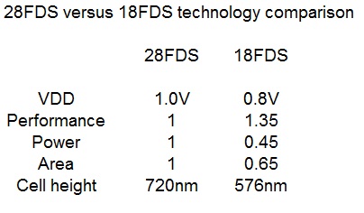
- 28FDS (FD-SOI) has been widely adopted, with a significant number of new tapeouts planned for 2019
- 28FDS added an embedded Magnetoresistive RAM (eMRAM) process module, introduced in 3/2019
- The plans for eMRAM will extend to the 18FDS node (with automotive grade qualification in 2020), and in the future, to FinFET nodes.
- 18FDS: PDK 0.5 was shipped in 9/2018, v1.0 available in 6/2019, Design Kit v1.0 in 12/2019
Here is a brief comparison between 28FDS and 18FDS.
RF
The timeline for RF design enablement for mmWave applications (e.g., 5G) is depicted below.
In addition, Samsung Foundry indicated they are focusing on providing analog and RF design services, at a range of potential interfaces with customers – Level0: spec handoff; Level1: architecture handoff; Level2: IP porting.
Packaging
In addition to the semiconductor process node and 3GAE introduction, Samsung Foundry presented the breadth of their advanced 2.5D and fan-out packaging technologies. The FO packaging offering is based on Samsung’s unique “panel-level” form factor (FO-PLP). The 2.5D multi-die offering provides integration of logic and HBM modules with an interposer.
3GAE
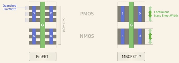
The big announcement was the availability of PDK v0.1 for the 3nm process node (3GAE), by Dr. H.K. Kang, EVP, Samsung Semiconductor R&D Center. This node transitions from vertical FinFET devices to a gate-all-around implementation, a structure that Samsung Foundry denotes as a “Multi-Bridge Channel FET” (MBCFET). The figure below from Samsung Foundry provides a high-level depiction of the GAA device.
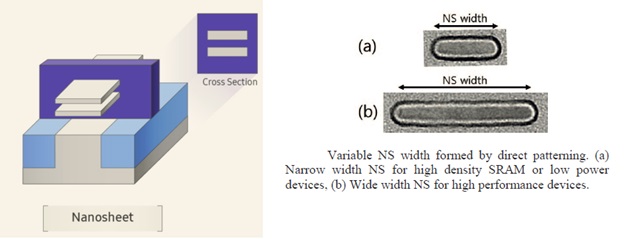
Note that there are multiple, horizontally-oriented “nanosheets” stacked vertically, with a surrounding gate electrode – the effective device width would be (2*(thickness + width) * # of sheets). (The Samsung Foundry presentations were a little vague on the specific 3GAE implementation – there were different slide images depicting 2, 3, and 4 vertical nanosheets.) Of specific note is that the GAA device width is now a design parameter, enabling a wider range of design optimizations.
The figure below illustrates how a FinFET layout (3 fins) compares to a GAA implementation – unlike the quantized height of the active area associated with the fins, the width of the nanosheets is a design variable.
The PPA comparisons from 7nm to 3GAE were impressive (using Ion-versus-Ioff type data): +35% performance, -50% power (@ iso perf., -40% power at fmax), -45% area.
With the improved channel electrostatics of the gate-all-around topology, the subthreshold slope data presented was impressive. The supply voltage VDD for 3GAE will scale to 0.7V.
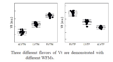
The 3GAE presentation described three device Vt offerings: RVT (~0.35V); LVT (~0.25V), and SLVT (~0.15V) – refer to the figure below. The Pelgrom chart of deltaVt versus (gate_area **0.5) showed comparable Vt mismatch variation to FinFET offerings. Dr. Kang indicated, “Samsung Semiconductor R&D has been working on GAA technology for some time. The most difficult process integration step was to develop the replacement gate technology to provide multiple Vt offerings.”
See patent #US7002207, culminating in the IEDM 2018 technical paper: Bae G., et al., “3nm GAA Technology featuring Multi-Bridge-Channel FET for Low Power and High Performance Applications”, International Electron Devices Meeting (IEDM), 2018, p. 28.7.1 – 28.7.4. The figure below is from that paper, highlighting the use of different work function metals to provide the Vt options.
Similarly, the local deltaT temperature increase due to device self-heating was comparable to FinFET topologies. Bias temperature instability (BTI) drive over time was similar, as well.
Design enablement for the 3GAE process was announced, as part of the v0.1 PDK release to customers. Specifically, SPICE models will continue to utilize the BSIM-CMG compact model format, which includes a gate-all-around topology. (Kudos to the Berkeley Device Model group for anticipating that the GAA electrostatic model would be needed.) Place-and-route techfiles, pCells, and fill algorithms for layout implementation were released. Parasitic extraction, DRC, and LVS runsets were also part of the v0.1PDK release.
As an aside, the parasitic capacitances for the GAA device will certainly differ from FinFETs. The Cgs and Cgd sidewall parasitics for the gate traversing between fins are now reflected in the gate between the stacked nanosheets. The spacing between nanosheets is a critical process optimization parameter – refer to the IEDM paper cited above. The Cgx capacitance for the gate-over-substrate between fins is replaced by the capacitance to substrate of the gate below the bottom nanosheet. The extracted gate resistance element, Rg, will also differ for the unique GAA cross-section. (I’m planning on investigating the BSIM-CMG model for a GAA topology in more detail.)
Both 3GAE and 3GAP node introductions were presented on the process roadmap in the figure above. As mentioned above, the v0.1 PDK release for 3GAE is available now. The 3GAE node will enter risk production in late 2020, with HVM in late 2021. (In my notes, I have written that the 3GAP dates will be roughly one year later.)
SAFE
Samsung Foundry also briefly described their “SAFE” program (Samsung Advanced Foundry Ecosystem), listing 16 EDA partners, 27 IP providers, and 27 design services solutions partners to assist customers. As mentioned above, the ecosystem for (hybrid) cloud-based design was also introduced, utilizing the resources and expertise of AWS and Azure, and a collaboration with Cadence and Synopsys.
The first “SAFE” event highlighting the breadth of this partnership will be held in Silicon Valley on 10/22/2019.
When describing the recent collaboration with the EDA vendors, there was one example presented that caught my attention. There’s been a lot of discussion on “how would machine learning principles apply to EDA algorithms” – an example was presented that I thought was extremely innovative. The mask house currently employs a sophisticated set of Source-Mask Optimization (SMO) algorithms to realize a printable mask. There is a risk that a layout topology may be unresolvable during SMO analysis. Although the goal is to exclude any problematic layout topologies as part of the DRC design rule checking runset, the foundries have introduced the additional requirement for designers to execute a Lithography Process Checking (LPC) flow. Initial LPC product releases integrated both model-based and pattern matching-based algorithms, to explore the layout for potential issues. The model-based analysis is comprehensive but very computationally expensive. The pattern matching approach is fast, but is “reactive”, in that it relies upon a set of patterns that have previously been identified. Samsung Foundry and Mentor Graphics have integrated a set of algorithms into Calibre LPC that apply machine learning techniques to extend the scope of “litho hot spot” layout analysis beyond the provided pattern library, without the computational complexity of detailed model-based analysis – very cool.
Reference: Kim, et al., “Machine learning to improve accuracy of fast lithographic hotspot detection”, SPIE, paper 10962-41, February 24-28, 2019.
Summary
Although in some regards Samsung Foundry is still “very young”, it was clear throughout the forum presentations that they are focused on execution of the existing process roadmap and are attempting to make a significant leap into the next generation device topology beyond vertical FinFETs. The use of GAA technology will relax some of the design restrictions associated with the “quantized” FinFET device width, and the 3GAE process node PPA comparisons to existing nodes were extremely compelling. Moore’s Law marches on.
For an overview of the 3GAE process node announcement, please refer to the following Samsung Foundry web link.
-chipguy
Share this post via:


Comments
4 Replies to “Samsung Foundry Update 2019”
You must register or log in to view/post comments.