
Last month in Shanghai was a meeting of the FD-SOI consortium. The focus of the meeting was largely on the suitability of using FD-SOI to serve the Chinese market. The fabs in China are not right on the bleeding edge and are very cost-sensitive so 28nm is probably as advanced as they will get for a long time if not indefinitely. China … Read More
 Enhancing the RISC-V Ecosystem with S2C Prototyping SolutionRISC-V's popularity stems from its open-source framework, enabling…Read More
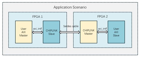
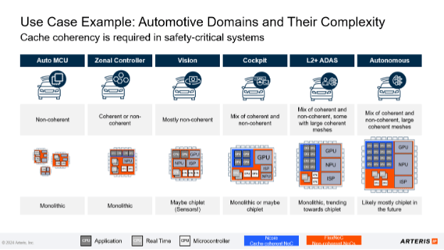 Arteris Frames Network-On-Chip Topologies in the CarOn the heels of Arm’s 2024 automotive update,…Read More
 LIVE WEBINAR: Automating the Integration Workflow with IP Centric DesignSubsystem and full-chip integration plays a crucial role…Read More
 The Data Crisis is Unfolding – Are We Ready?The rapid advancement of technology, including generative AI,…Read More
In-Design DFM Signoff for 14nm FinFET Designs

While FinFET yield controversy is going on, I see a lot being done to improve that yield by various means. One prime trend today, it must be, it’s worthwhile, is to pull up various signoffs as early as possible during the design cycle. And DFM signoff is a must with respect to yield of fabrication. This reminds me about my patents filed… Read More
Its a bouncing baby IEEE standard!

Pass the cigars! On November 3rd, 2014, the IEEE-SA Standards Board finally approved IEEE P1687 as a new standard. From now on, you can drop the “P” and just call it 1687, or to its friends, IJTAG. Now would be a good time to sign up for an IJTAG technical workshop.
The new IEEE 1687 Internal JTAG (IJTAG) standard is changing… Read More
Improve Test Robustness & Coverage Early in Design
In a semiconductor design, keeping the design testable with high test coverage has always been a requirement. However with shrinking technology nodes and large, dense SoC designs and complex logic structures, while it has become mandatory to reach close to 100% test coverage, it’s extremely difficult to cope with the explosion… Read More
Let the FinFET Yield Controversy Begin!
It never ceases to amaze me how people point fingers and create controversy to cover their mistakes. It happened at 40nm, 28nm, and again at 20nm and now it is time for the regularly scheduled yield controversy. Of course any conversation about semiconductor yield generates clicks for SemiWiki so I’m happy to play along.
It generally… Read More
DAC Deadlines: Action This Day
DAC is coming up. OK, it’s not actually until next June. It is June 7-11th 2015 at the Moscone Center here in San Francisco. But there are lots of important deadlines coming up for papers, panels and more. The 52[SUP]nd[/SUP] DAC will focus on five key tracks:
- automotive
- IP design
- embedded systems
- hardware/software security
Semiconductor IP Forecast 2014 – 2020
Given that the majority of my 30+ years in Silicon Valley has revolved around semiconductor IP it should be of no surprise that IP is a big part of SemiWiki and our first book “Fabless: The Transformation of the Semiconductor Industry”. That is also why one of my first round blogger draft choices was IP expert Dr. Eric Esteve. Eric has… Read More
What Presentations to Attend During IP-SoC 2014 ?

Will you go to Grenoble next week to attend to IP-SoC? I will do it and will certainly listen to these Keynote Talks:
- “Platform IP: the next wave for SOCs from IoT to Datacenter” by Tony King-Smith, Executive Vice President, Marketing , Imagination Technologies
- “From Server-class to IoT SoCs: Enabling System
Noise & Reliability of FinFET Designs – Success Stories!
I think by now there has been good level of discussion on FinFET technology at sub-20 nm process nodes and this is an answer to ultra dense, high performance, low power, and billion+ gate SoC designs within the same area. However, it comes with some of the key challenges with respect to power, noise and reliability of the design. A FinFET… Read More
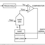
Debugging a 10 bit SAR ADC
SMIC (Semiconductor Manufacturing International Corporation) is a China-based foundry with technology ranging from 0.35 micron to 28 nm, and we’ve blogged about them before on SemiWiki. I’ve been reading about SMIC recently because they created a technical presentation for the MunEDA Technical Forum Shanghai… Read More
The Data Crisis is Unfolding – Are We Ready?