Array
(
    [content] => 
    [params] => Array
        (
            [0] => /forum/index.php?threads/wafer-size-fab-processing-questions.15318/
        )

    [addOns] => Array
        (
            [DL6/MLTP] => 13
            [Hampel/TimeZoneDebug] => 1000070
            [SV/ChangePostDate] => 2010200
            [SemiWiki/Newsletter] => 1000010
            [SemiWiki/WPMenu] => 1000010
            [SemiWiki/XPressExtend] => 1000010
            [ThemeHouse/XLink] => 1000970
            [ThemeHouse/XPress] => 1010570
            [XF] => 2021370
            [XFI] => 1050270
        )

    [wordpress] => /var/www/html
)

Wafer size / fab processing questions

jms_embedded

Active member
I have a question about the impact of wafer size on fab processing. I understand the general idea that larger wafers can improve throughput, but there's some nuances that seem to get glossed over. (hmm I can't seem to make a bulleted list in this post)
  • Lithography: area per unit time is constant, so larger area doesn't improve throughput without making the tools faster
  • Other steps: Which are constant time (more throughput if you can fit more wafer area in the tool) and which are bounded by area per unit time like lithography?
  • Wafer utilization: larger wafers mean that unusable area at the edge will be a smaller fraction of the total area, although when you can fit 5000 die on a 300mm wafer this effect is small, and would have more significant benefit for larger die (> 10mm x 10mm)

Is the bottleneck to 450mm wafers due more to the tools needing to be redesigned to fit 450mm wafers, or some inherent practical mechanical limitation of the wafer size itself? (weight/thickness/brittleness/flexing of large diameter wafers) Is there a reason we don't have arrays of smaller wafers instead of a single larger wafer? Not an ideal situation in space-constrained tools, but if the issue has to do with something about 450mm wafers that aren't practical due to mechanical issues, it seems like increasing the area that gets processed simultaneously is a slightly different goal than increasing the area of the wafer itself.
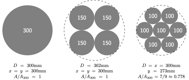
wafers-question.png
 
It's not that big of a problem to manufacture a roughly 2 times heavier wafer stage. It's a problem to nudge the whole of material handling industry.

EUV was supposed to be the incentive to go to 450, because vacuuming the chamber every time new wafer is coming is costly, but that was solved with wafer magazines inside the tool, just like with deposition tools.
 
jms, there many elements to consider here. Here are a few.

1- Cutting edge tools are only available on 300 mm. There is no EUV on 200 mm for example.
2- You are neglecting the impact of wafer edge. The usable area for a 300 mm is approximately 292 mm (varies from fab to fab). Using the same exclusion, your 100 mm is now 92 mm (there is the related issue of clamping which is too technical to discuss here but critical as it makes large edge exclusions)
3- You are neglecting the time of handling. Many process handling steps are relying on gravity to hold the wafer in place. This means that the maximum acceleration is about 0.3g. In practice, this means that the handling time does not scale with wafer size. That strongly favors 300 mm.
4- The lot size is a significant factor that cut both ways. In 200 mm factories, the "lot" is an entire cassette. i can place 1 wafer in the cassette or I can put the full 25. In 300 mm, I can have multiple lots within the same cassette. Depending on die size, some products will be more cost effective on 200 mm, others on 300 mm. You can see that at 450, even with a single wafer, the lot size would be gigantic (at least for small dies).
5- Not a single company can afford to finance a wafer size change. It's like the three musketeers. All for one, one for all. Think about all the OEMs, all the OPMs, etc. 450 may have been marginally more cost effective on paper but not affordable for anyone bar possibly the big 3 (acting together and obsoleting 300 mm at the same time). In practice, more could be (and was) done with EUV on 300 mm than could be done with 450 mm (IMO). Think A380. Kind of similar.

Bottom line: Under 100 mm = R/D only. 100 mm = specialty factories, special wafers (sapphire, selenium, etc.). 150 mm = rapidly going to SiC. 200 mm = large and growing very slowly - main issue many OEMs either are gone or no longer support. 300 mm = nearly all new factories. 450 mm = never
 
OK thank you for the clarification. So what I'm hearing is that in addition to constant area per time (lithography) and batch per time (other processes) there are a couple of major issues:

- area usability of larger wafers is a few percent larger, because of unusable edge (your point #2)

- network effects: ecosystem will support whatever everybody shifts to, but it takes enormous investments to make any shift (this covers your points 1 and 5)

...and I don't hear anything that is really a negative about the larger wafers 300mm or 450mm based on physics/geometry alone except for perhaps points 3 and 4.

Point 4:
In 200 mm factories, the "lot" is an entire cassette. i can place 1 wafer in the cassette or I can put the full 25. In 300 mm, I can have multiple lots within the same cassette.
Why aren't 200mm and 300mm wafers subject to the same rules?

Point 3: "time of handling", acceleration <= 0.3g, handling time doesn't scale... could you elaborate on how this works? Meaning larger wafers are worse or better?

200 mm = large and growing very slowly - main issue many OEMs either are gone or no longer support.
...and this is a separate point from my main question, but is a somewhat scary tension, if the demand is going up but the interest in providing more supply (from the equipment manufacturers) is not.
 
On point #4. They are subject to the same rule. It takes about the same amount of time to move a 200 mm and a 300 mm wafer from A to B. So 300 mm is more cost effective in terms of "square inches of silicon moved per unit of time" (in terms of handling). Same for overhead handling. At constant speed, 300 mm is more cost effective.

Your last comment rephrased: could we ever see a big revival of 200 mm? Frankly not. You will see "still-in-business" OEMs sell new 200 mm tools (AMAT, TEL, LAM are doing it). Not much however can be done for companies that no longer exist. Then you have the issue of old-tech vs new tech. There will not be new tech on 200 mm (SiC or sapphire is another story). These forces explain 2 things: very large capex from big companies (TSMC, Intel, Samsung, Micron etc): it's all 300 mm and complicated and declining market share for companies still exclusively on 200 mm. Some 200 mm LED factories will be converted to silicon. What has been missing are "low-tech" 300 mm fabs (say 90 nm). On Semi Fishkill will be one such factory and you could say that the TI fabs are low-tech (they are not but they are analog so less complicated in many ways). 300 mm costing what it does, it makes no financial sense to go trailing edge. Could change with bankruptcies (See Qimonda, Micron UT) but the demand for chips is such that everyone is making money so no imminent financial black swan.
 
I have a question about the impact of wafer size on fab processing. I understand the general idea that larger wafers can improve throughput, but there's some nuances that seem to get glossed over. (hmm I can't seem to make a bulleted list in this post)
  • Lithography: area per unit time is constant, so larger area doesn't improve throughput without making the tools faster
  • Other steps: Which are constant time (more throughput if you can fit more wafer area in the tool) and which are bounded by area per unit time like lithography?
  • Wafer utilization: larger wafers mean that unusable area at the edge will be a smaller fraction of the total area, although when you can fit 5000 die on a 300mm wafer this effect is small, and would have more significant benefit for larger die (> 10mm x 10mm)

Is the bottleneck to 450mm wafers due more to the tools needing to be redesigned to fit 450mm wafers, or some inherent practical mechanical limitation of the wafer size itself? (weight/thickness/brittleness/flexing of large diameter wafers) Is there a reason we don't have arrays of smaller wafers instead of a single larger wafer? Not an ideal situation in space-constrained tools, but if the issue has to do with something about 450mm wafers that aren't practical due to mechanical issues, it seems like increasing the area that gets processed simultaneously is a slightly different goal than increasing the area of the wafer itself.

View attachment 619
There are basically two classes of tools, beam tools and non-beam tools. Beam tools scan the wafer; exposure, implant and some inspection and metrology tools are beam tools. All other fab tools are non-beam tools.

For beam tools throughput is more complex than you are considering because there is wafer level overhead and then the scan time. For exposure tools wafer overhead can be significant, especially for EUV tools with low output beams.

For non-beam tools the wafers per hour (wph) throughput is largely independent of wafer size.

When 450mm was being worked on there was an acknowledgment that the beam tools were going to be slower for 450mm than for 300mm because beam current density is reaching fundamental limits particularly for implant. Even accounting for that, 450mm was going to provide an overall cost reduction in per wafer cost. At the end of the day the investment required was so high that the industry decided to focus on other issues. 450mm required all new tools and even new fabs because of the tool size. No one had the stomach to retool the entire industry.

The 300mm transition saw a clean sheet tool design approach. Only a small number of 200mm fabs were minienvironments, all 300mm fabs are. 200mm fabs had bay to bay automation but not within the bay. All 300mm tools are designed so that overhead transport systems can deposit wafers right onto the tool. Ironically, for 300mm the tools are all designed so that multiple input FOUPs can be loaded at the same time so that the tools don't run out of wafers, this resulted in an increase in cycle time for 300mm because more wafers were waiting to be processed. This surprised a lot of people although it was entirely predictable from a manufacturing science perspective.

A lot of work was done on uptime and throughput for 300mm tools, in fact 300mm exposure tools very quickly exceeded 200mm exposure tool wph and the wph is still going up. There was a time when 60 wph was good throughput for a 200mm exposure tool, today we are closing in on 300 wph for 300mm exposure tools.

A lot of the 300mm improvements could be implemented for 200mm but that would be a very expensive undertaking for the equipment companies, and they don't see the payback. In fact, historically each wafer size conversion has seen improvements on the existing wafer size stop quickly once the new wafer size is implemented. 150mm tools aren't generally designed for less than 800nm processing and 200mm tools aren't generally designed for less than 130nm processing.
 
Aha, now we're getting somewhere. Thanks both of you for the informative responses. (Part of my confusion is terminology! If I know what to search for, at least there's some hope of finding a technical article somewhere.)

On point #4. They are subject to the same rule. It takes about the same amount of time to move a 200 mm and a 300 mm wafer from A to B. So 300 mm is more cost effective in terms of "square inches of silicon moved per unit of time" (in terms of handling). Same for overhead handling. At constant speed, 300 mm is more cost effective.

OK, so you're talking motion between tools? (Or similar motion-related constraints within a tool) I can see the cost-effectiveness for some movements if the motion is restricted to one wafer at a time for some reason (example if a tool has to pick up or rotate or place exactly one wafer). But I think I'm lost if we're talking about "lot size" = a group of wafers in a carrier (FOUP or other)... nine 200mm wafers have the same area (aside from a few percent in edge effects) as four 300mm wafers, so if each of them contains the same number of dice, why wouldn't they be equally attractive in this sense?

What has been missing are "low-tech" 300 mm fabs (say 90 nm)

Yes, I guess that was my mistake of conflating "demand for 200mm" with "demand for mature nodes" -- the articles on the subject don't seem to clearly distinguish the difference. I follow the idea that if someone's going to add new capacity for mature nodes, better to do so at 300mm than 200mm.

300 mm costing what it does, it makes no financial sense to go trailing edge.

Then that's the scary part.... today's capacity for "mature nodes" has been paid for in years past, when the equipment was were leading-edge and demanded a premium, and the market was able to pay for the depreciation. Now that demand has increased due to IoT/automotive/low-end microcontrollers --- and I'm fuzzy on the economics but my vague understanding is that there are engineering reasons that drive new designs on >= 40nm even though the cost per digital transistor is greater than at 28nm or less --- what happens if the economic pressure from that demand isn't enough to justify adding brand-new equipment at these nodes, whether it's 200mm or 300mm? Is the supply/demand mismatch in capacity on mature nodes destined to continue for years?

I'm hoping I'm missing some simple point, and it'll just be some combination of ways to bring relief to the situation: some designs are migrated to 16nm/20nm/22nm/28nm, which is what TSMC and Intel seem to be hoping; some designs stay on existing older capacity; some designs get put on new 300mm equipment for older nodes brought up by TI (Lehi UT + new TX fabs) or ON Semi (Fishkill) or Infineon (Villach, Austria) or Bosch (Dresden) or some of the Chinese foundries; or some of the demand goes away.

There are basically two classes of tools, beam tools and non-beam tools. Beam tools scan the wafer; exposure, implant and some inspection and metrology tools are beam tools. All other fab tools are non-beam tools.

Thank you, the terminology + summary helps me understand.

For beam tools throughput is more complex than you are considering because there is wafer level overhead and then the scan time. For exposure tools wafer overhead can be significant, especially for EUV tools with low output beams.

Is there a simple reason for that? (and is this something that I can find out myself reading something on ASML's website or in a technical paper? or it's details that you wouldn't run into until you're involved directly with an EUV fab?) Paul2 mentioned this:

EUV was supposed to be the incentive to go to 450, because vacuuming the chamber every time new wafer is coming is costly, but that was solved with wafer magazines inside the tool, just like with deposition tools.

For non-beam tools the wafers per hour (wph) throughput is largely independent of wafer size.

There is a nuance here (for non-beam tools) that I am trying to wrap my head around. namely the following points:

A. What drives a tool to have an inherent affinity for working with a single wafer at a time? (For example, if etching is a non-beam tool, and it takes, say, 30 minutes to run some process step on one wafer, why wouldn't someone make a tool that processes four wafers simultaneously to improve throughput per unit machine cost?)

B. If there *isn't* an affinity for working with a single wafer, do 300mm wafers really have much cost advantage over 200mm wafers for these tools? (example: imagine Tool X variety A can process nine 200mm wafers, but Tool X variety B can process four 300mm wafers, for about the same wafer area throughput)

C. Or do 300mm wafers get about the same # of wafers/hour in tools, simply because the money is there to finance that level of performance through new tool design, and it isn't for 200mm wafer tools? (in other words, if you could buy a new Tool X variety A that could process four 300mm wafers per hour, the manufacturer could just as easily design Tool X variety B that could process nine 200mm wafers per hour for technical reasons, but the money isn't there to pay for variety B)
 
"Thank you, the terminology + summary helps me understand."

Beam tools is a classification that came out of the 450mm work, if you can find some of the old articles they talk about it.

"Is there a simple reason for that? (and is this something that I can find out myself reading something on ASML's website or in a technical paper? or it's details that you wouldn't run into until you're involved directly with an EUV fab?)"

Its the kind of thing you likely wouldn't run across unless you worked on steppers in a fab. All steppers (not just EUV) load a wafer, do metrology and set up (wafer level overhead) and then start stepping and exposing. The wafer needs to be level, in focus, and the steppers needs to know the exact positions to expose with nanometer resolution, it is incredibly hard to do. DUV steppers have higher light intensity (beam current) and expose after each step faster than EUV so wafer overhead is less of a factor, but it matters. Harry Levinson has the throughput formula in his lithography book, of course to use the formula you need to know what to plug in for numbers and that information is ASML proprietary, I have good estimates but it is not something I am willing to share.

"Paul2 mentioned this: Paul2 said: EUV was supposed to be the incentive to go to 450, because vacuuming the chamber every time new wafer is coming is costly, but that was solved with wafer magazines inside the tool, just like with deposition tools."

The rational for 450mm was to reduce cost in general, it wasn't specifically EUV driven (I disagree with his statement). In fact 450mm would have reduced the cost per square centimeter of silicon but the overall investment to get there was just too big. I published several articles on 450mm back in the 2010 to 2014 time frame including costs versus 300mm and I consistently found it was less expensive.

Almost all leading edge processing is done in single wafer chambers today in order to achieve the control required. If 200mm tools existed to make 3nm logic they would primarily be single wafer as well. The industry over its history has trended to more automation, more single wafer processing, and larger wafer sizes all in parallel.

For many operations such as deposition or etch there is a rate that determines the time to process a wafer, for example if you can deposit 10nm per minute, if you are depositing 100nm it is 10 minutes regardless of wafer size. Some 3D NAND etches are 60+ minutes per wafer!

Most fab equipment these days are cluster tools with central input and output stations, one or two central robots and multiple process stations with cleans, depositions, curing, metrology, etc. all while still under vacuum. Throughput on these system is unbelievably complex to understand and model. I once spent months working on a throughput model with an expert at one of the leading equipment manufacturers. To think about it simply, just remember that each chamber is limited by the rate and the wafers per hour per chamber is independent of wafer size, bigger wafers equal more silicon area per hour per chamber. For some 3D NAND operations there are cluster tools with 16 wafer positions processing wafers simultaneously.

I am going to bow out of this discussion now as this is all the time I can devote to it. This is the kind of subject that would take a book length write up to fully explore. Good luck!
 
I published several articles on 450mm back in the 2010 to 2014 time frame including costs versus 300mm and I consistently found it was less expensive.

I found some of those when searching for "beam" and "non-beam" earlier today. (450mm is yet another rabbit hole to get lost in....)

Thank you so much -- that gives me a flavor of what's going on, and that's all I was looking for. (Well, of course I'm curious for more, but I'll take whatever crumbs I can get :) )

I am going to bow out of this discussion now as this is all the time I can devote to it. This is the kind of subject that would take a book length write up to fully explore. Good luck!

Is this something you've got in mind when you retire? ;) I'll buy a copy.
 
...and from the Trust-But-Verify Department:

memsstar article: Single Wafer vs Batch Wafer Processing
In both semiconductor device and microelectromechanical systems (MEMS) manufacturing, wafer processes are generally divided into single wafer and batch processing. As the name implies, batch processing calls for multiple wafers to be processed at the same time. This cost-effective approach is typically used for thermal oxidation, low pressure chemical vapor deposition (LPCVD) of silicon nitride, resist strips and wafer cleaning processes.

Recently, however, tightening requirements to achieve finer features is driving a need for high quality deposition and etch processes. As a result, there has been a significant shift towards single wafer processing. The main considerations of a batch vs single wafer approach are reviewed here, highlighting reasons where one method may be preferred over another.


Veeco article:
The Application Specific Evolution of Single Wafer Wet Etch Tools
Specifying the correct etch tool is an application specific process. Automated wet etch originated in bench systems. While inexpensive and offering high throughput, these systems suffered from poor process control within wafer, wafer to wafer and lot to lot. There were signatures from the etch process based on position in the cassette and wafer orientation. Open bath systems were high in defectivity, chemical usage, waste creation and open baths were a safety hazard. Batch spray systems maintained high throughput and offered better process control compared to a wet bench but still suffered from non-optimal performance. Single wafer emerged as the technology to permit each wafer to see the same process and obtain identical results. The advantages of single wafer were clear: best uniformity, highest repeatability, lowest defectivity processes. These results were obtained within a safe toolset that offered low chemical usage and minimal waste creation.
 
@Scotten Jones Excellent background information. The 450 tools were gigantic indeed for those of luck lucky enough to see them. RIP. Yes it was going to be cheaper on paper but it was far from clear that all OPMs would be able to join. I fear that we would have ended up like FPD with 2 or 3 OEMs and no second-source suppliers. At any rate, that is in the past.

@jms_embedded There is a point that needs to be very clear in your mind (restated from your own links). Nearly ALL 300 mm tools process wafers ONE AT A TIME. To get around the inherent time limitation (of process time and handling), multiple chambers running the same process will be clustered around a central robot. Going all the way back to 4" (it was not metric then), nearly all wafers were processed in batches, that meant an entire cassette or even multiple cassettes at one time. On top of the obvious issue of chamber size scaling, single wafer processing affords an immense amount of control over wafer placement, deposition and etch uniformity, temperature etc. That level of control is necessary for leading edge. Moreover, a dirty chamber will only ruin a single wafer (if you can catch it). A batch processor will ruin the entire lot. (There is an important exception in 300 mm: diffusion).

@jms_embedded In terms of area of silicon per unit of time (for handling) - A 300 mm wafer physically moves many times when going from A to B to C. In step 1, it moves on an overhead handling within a FOUP (a cassette). That FOUP is lifted from tool A, goes on a rail and is dropped on tool B. In step 2, the FOUP is open and a buffer robot (aka FI robot for factory interface) picks up each wafer, ONE AT A TIME and delivers it to the tool (in reality, the distance is minimal). Step 3 The wafer is them picked up by a second robot (often called transfer but could be buffer) and delivered to a chamber for processing. There could be multiple sequential steps at that time. In step 4, the same transfer robot delivers the wafer back to the FI robot which reloads the wafer to the FOUP which will be picked up to leave tool B. All of that handling takes time and is more or less independent of wafer size for reasons explained earlier. So the same configuration in 200 mm would deliver a lot less area of silicon per hour compared to 300 mm.

How do we get out of the shortage environment we are in? If you consider that it is nearly all low-tech (say 90 nm or above), then it means either companies porting old designs to 45 nm or below or building new factories that are 300 mm but low tech. I do not believe in low tech 300 mm (outside of repurposing banktrupt fabs) so you are left with porting. Automotive companies were (are) notorious for blocking change (in fab location, in tool location and even more so in wafer size and geometry). Bottom line, some kind of non-uniform shortage is here to stay although elimination of WFO and all things crypto would help.

I add here an ironical observation. 300 mm is very expensive as a development platform, especially for processes that do not yet exist. For all R&D outfits, a lot of the initial research will be done on small wafers or even on wafer fragments. Selective ALD Cobalt (example) would have been developed and validated on small Si pieces before the OEM was tasked with porting it to an actual tool...
 
Back
Top